
Datasheet


STM32F050xx Electrical characteristics
Doc ID 023683 Rev 1 37/97
6.2 Absolute maximum ratings
Stresses above the absolute maximum ratings listed in Table 12: Voltage characteristics,
Table 13: Current characteristics, and Table 14: Thermal characteristics may cause
permanent damage to the device. These are stress ratings only and functional operation of
the device at these conditions is not implied. Exposure to maximum rating conditions for
extended periods may affect device reliability.
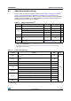
Table 12. Voltage characteristics
(1)
1. All main power (V
DD
, V
DDA
) and ground (V
SS
, V
SSA
) pins must always be connected to the external power
supply, in the permitted range.
Symbol Ratings Min Max Unit
V
DD
–V
DDA
Allowed voltage difference for V
DD
>V
DDA
-0.4V
V
IN
(2)
2. V
IN
maximum must always be respected. Refer to Table 13: Current characteristics for the maximum
allowed injected current values.
Input voltage on FT and FTf pins V
SS
− 0.3 V
DD
+ 4.0 V
Input voltage on TTa pins V
SS
− 0.3 4.0 V
Input voltage on any other pin V
SS
− 0.3 4.0 V
|ΔV
DDx
| Variations between different V
DD
power pins - 50 mV
|V
SSX
− V
SS
|
Variations between all the different ground
pins
-50mV
V
ESD(HBM)
Electrostatic discharge voltage (human
body model)
see Section 6.3.11: Electrical
sensitivity characteristics
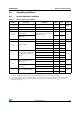
Table 13. Current characteristics
Symbol Ratings Max. Unit
I
VDD(Σ)
Total current into sum of all VDD_x
and VDDSDx power lines
(source)
(1)
120
mA
I
VSS(Σ)
Total current out of sum of all VSS_x
and VSSSD ground lines
(sink)
(1)
-120
I
VDD(PIN)
Maximum current into each VDD_x or VDDSDx power pin (source)
(1)
100
I
VSS(PIN)
Maximum current out of each VSS_x or VSSSD ground pin (sink)
(1)
-100
I
IO(PIN)
Output current sunk by any I/O and control pin 25
Output current source by any I/O and control pin - 25
ΣI
IO(PIN)
Total output current sunk by sum of all IOs and control pins
(2)
80
Total output current sourced by sum of all IOs and control pins
(2)
-80
I
INJ(PIN)
Injected current on FT, FTf and B pins
(3)
-5/+0
Injected current on TC and RST pin
(4)
± 5
Injected current on TTa pins
(5)
± 5
ΣI
INJ(PIN)
Total injected current (sum of all I/O and control pins)
(6)
± 25
1. All main power (VDD, VDDA) and ground (VSS, VSSA) pins must always be connected to the external power supply, in the
permitted range.