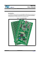
UM1658 User manual Discovery kit for STM32F030 Value Line microcontrollers Introduction The STM32F030 Value Line Discovery kit (32F0308DISCOVERY) helps you to discover the device features and to develop your applications easily. It is based on STM32F030R8T6, an STM32 F0 series 32-bit ARM® Cortex™-M0 microcontroller, and includes an ST-LINK/V2 embedded debug tool, LEDs, push buttons and a prototyping board. Figure 1. 32F0308DISCOVERY September 2013 DocID025097 Rev 1 1/39 www.st.
Contents UM1658 Contents 1 Conventions . . . . . . . . . . . . . . . . . . . . . . . . . . . . . . . . . . . . . . . . . . . . . . . . 5 2 Quick start . . . . . . . . . . . . . . . . . . . . . . . . . . . . . . . . . . . . . . . . . . . . . . . . . 6 2.1 Getting started . . . . . . . . . . . . . . . . . . . . . . . . . . . . . . . . . . . . . . . . . . . . . . 6 2.2 System requirements . . . . . . . . . . . . . . . . . . . . . . . . . . . . . . . . . . . . . . . . . 6 2.
UM1658 List of tables List of tables Table 1. Table 2. Table 3. Table 4. Table 5. Table 6. Table 7. Table 8. Table 9. Table 10. Table 11. ON/OFF conventions . . . . . . . . . . . . . . . . . . . . . . . . . . . . . . . . . . . . . . . . . . . . . . . . . . . . . . 5 Jumper states . . . . . . . . . . . . . . . . . . . . . . . . . . . . . . . . . . . . . . . . . . . . . . . . . . . . . . . . . . . 13 Debug connector CN3 (SWD) . . . . . . . . . . . . . . . . . . . . . . . . . . . . . . . . . . . . . . . . .
List of figures UM1658 List of figures Figure 1. Figure 2. Figure 3. Figure 4. Figure 5. Figure 6. Figure 7. Figure 8. Figure 9. Figure 10. Figure 11. Figure 12. Figure 13. Figure 14. Figure 15. Figure 16. 4/39 32F0308DISCOVERY . . . . . . . . . . . . . . . . . . . . . . . . . . . . . . . . . . . . . . . . . . . . . . . . . . . . . 1 Hardware block diagram . . . . . . . . . . . . . . . . . . . . . . . . . . . . . . . . . . . . . . . . . . . . . . . . . . . 8 Top layout . . . . . . . . . . . . . . . . .
UM1658 1 Conventions Conventions Table 1 provides the definition of some conventions used in the present document. Table 1.
Quick start 2 UM1658 Quick start The STM32F030 Value Line Discovery kit is a low-cost and easy-to-use development kit to quickly evaluate and start development with an STM32 F0 series microcontroller. Before installing and using the product, please accept the Evaluation Product License Agreement from www.st.com/stm32f0-discovery. For more information on the STM32F030 Value Line Discovery kit and for demonstration software, visit www.st.com/stm32f0-discovery. 2.
UM1658 3 Features Features The STM32F030 Value Line Discovery kit offers the following features: • STM32F030R8T6 microcontroller featuring 64 KB Flash, 8 KB RAM in an LQFP64 package • On-board ST-LINK/V2 with selection mode switch to use the kit as a standalone ST-LINK/V2 (with SWD connector for programming and debugging) • Board power supply: through USB bus or from an external 5 V supply voltage • External application power supply: 3 V and 5 V • Four LEDs: – LD1 (red) for 3.
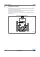
Hardware and layout 4 UM1658 Hardware and layout The STM32F030 Value Line Discovery board is designed around the STM32F030R8T6 microcontroller in a 64-pin LQFP package. Figure 2 illustrates the connections between the STM32F030R8T6 and its peripherals (ST-LINK/V2, push button, LEDs and connectors). Figure 3 and Figure 4 help you to locate these features on the STM32F030 Value Line Discovery board. Figure 2.
UM1658 Hardware and layout Figure 3. Top layout (red/green LED) LD2 COM LD1 (red LED) PWR ST-LINK/V2 5V power supply input output 3V power supply input output CN3 SWD connector CN2 ST-LINK/DISCOVERY selector JP2 IDD measurement SB1 (VDD) SB3 (B1-USER) B2 reset button STM32F030R8T6 SB4 (B2-RESET) B1 user button (green LED) LD3 LD4 (blue LED) MB1134 revA STM32F0308-DISCO MS31936V1 Note: Pin 1 of CN2, CN3, P1 and P2 connectors are identified by a square.
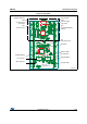
Hardware and layout UM1658 Figure 4.
UM1658 4.1 Hardware and layout STM32F030R8T6 microcontroller The STM32F030R8T6 microcontroller incorporates the high-performance ARM Cortex™-M0 32-bit RISC core operating at a 48 MHz frequency, high-speed embedded memories (up to 64 Kbytes of Flash memory and up to 8 Kbytes of SRAM), and an extensive range of enhanced peripherals and I/Os.
Hardware and layout UM1658 Figure 6. STM32F030R8T6 block diagram Serial Wire Debug VDD18 Obl Flash interface SWCLK SWDIO as AF SRAM controller NVIC Bus matrix CORTEX-M0 CPU fHCLK = 48 MHz Flash up to 64 KB, 32 bits SRAM 4 / 8 KB POWER VOLT.REG 3.3 V TO 1.8 V VDD = 2.4 to 3.
UM1658 4.2 Hardware and layout Embedded ST-LINK/V2 The ST-LINK/V2 programming and debugging tool is integrated on the 32F0308DISCOVERY. The embedded ST-LINK/V2 can be used in 2 different ways according to the jumper states (see Table 2): • Program/debug the MCU on board, • Program/debug an MCU in an external application board using a cable connected to SWD connector CN3. The embedded ST-LINK/V2 supports only SWD for STM32 devices.
Hardware and layout 4.2.1 UM1658 Using ST-LINK/V2 to program/debug the STM32 F0 on board To program the STM32 F0 on board, simply plug in the two jumpers on CN2, as shown in Figure 8 in red, but do not use the CN3 connector as that could disturb communication with the STM32F030R8T6 of the 32F0308DISCOVERY. Figure 8.
UM1658 4.2.2 Hardware and layout Using ST-LINK/V2 to program/debug an external STM32 application It is very easy to use the ST-LINK/V2 to program the STM32 on an external application. Simply remove the 2 jumpers from CN2 as shown in Figure 9, and connect your application to the CN3 debug connector according to Table 3. Note: SB19 and SB22 must be OFF if you use CN3 pin 5 in your external application. Table 3.
Hardware and layout 4.3 UM1658 Power supply and power selection The power supply is provided either by the host PC through the USB cable, or by an external 5 V power supply. The D1 and D2 diodes protect the 5 V and 3 V pins from external power supplies: 4.4 4.5 4.6 • 5 V and 3 V can be used as output power supplies when another application board is connected to pins P1 and P2. In this case, the 5 V and 3 V pins deliver a 5 V or 3 V power supply and power consumption must be lower than 100 mA.
UM1658 Hardware and layout 4.7 OSC clock 4.7.1 OSC clock supply PF0 and PF1 can be used as GPIO or as HSE oscillator. By default these I/Os are configured as GPIO, so SB16 and SB17 are closed, SB18 is open and R22, R23, C13 and C14 are not populated. An external HSE clock can be provided to the MCU in three ways: • • • 4.7.2 MCO from ST-LINK. From MCO of the STM32F103. This frequency cannot be changed, it is fixed at 8 MHz and connected to PF0-OSC_IN of the STM32F030R8T6.
Hardware and layout 4.8 UM1658 Solder bridges Table 4. Solder bridge settings Bridge State(1) Description OFF X2, C13, C14, R22 and R23 provide a clock. PF0, PF1 are disconnected from P1. ON PF0, PF1 are connected to P1 (R22, R23 and SB18 must not be fitted). SB6,8,10,12 (Default) ON Reserved, do not modify. SB5,7,9,11 (Reserved) OFF Reserved, do not modify. SB20,21 (X3 crystal) OFF X3, C15, C16, R24 and R25 deliver a 32 KHz clock. PC14, PC15 are not connected to P1.
UM1658 4.9 Hardware and layout Extension connectors The male headers P1 and P2 can connect the 32F0308DISCOVERY to a standard prototyping/wrapping board. STM32F030R8T6 GPI/Os are available on these connectors. P1 and P2 can also be probed by an oscilloscope, logical analyzer or voltmeter. Table 5.
Hardware and layout UM1658 Table 5.
UM1658 Hardware and layout Table 5.
Hardware and layout UM1658 Table 5.
UM1658 Hardware and layout Table 5.
Hardware and layout UM1658 Table 5.
UM1658 5 Connecting modules on the prototyping board Connecting modules on the prototyping board This section gives some examples of how to connect ready-to-use modules available from different manufacturers to the STM32F030 Value Line Discovery kit via the prototyping board included in the kit. Software examples, based on the connections described below, are available at www.st.com/stm32f0-discovery. 5.1 Mikroelektronica accessory boards Mikroelektronika, http://www.mikroe.
Connecting modules on the prototyping board UM1658 Table 7. Connecting using IDC10 Mikroelektronica IDC10 connector 26/39 32F0308DISCOVERY P0 GPIO PC0 GPIO OUTPUT (3.3V tolerant) P1 GPIO PC1 GPIO OUTPUT (3.3V tolerant) P2 GPIO PC2 GPIO OUTPUT (3.3V tolerant) P3 GPIO PC3 GPIO OUTPUT (3.3V tolerant) P4 GPIO PC4 GPIO OUTPUT (3.3V tolerant) P5 GPIO PC5 GPIO OUTPUT (3.
UM1658 Connecting modules on the prototyping board The Figure 10 illustrates the connections between the 32F0308DISCOVERY and the 2 connectors, IDC10 and mikroBUS™. Figure 10.
Connecting modules on the prototyping board 5.2 UM1658 ST MEMS “adapter boards”, standard DIL24 socket STMicroelectronics has defined a standard DIL24 connector to easily evaluate its MEMS sensors connected to a microcontroller through SPI or I2C communications. Table 8 is one solution for connecting the DIL24 boards to the 32F0308DISCOVERY, this solution is used in different examples and available at www.st.com/stm32f0-discovery. Table 8.
UM1658 Connecting modules on the prototyping board Figure 11 illustrates the connections between the 32F0308DISCOVERY and the DIL24 socket. Figure 11.
Connecting modules on the prototyping board UM1658 Supported MEMS adapter boards Table 9 is a list of supported MEMS adapter boards as of April, 2012. Table 9.
UM1658 Connecting modules on the prototyping board Table 9. Supported MEMS adapter boards (continued) ST MEMS DIL24 Eval Board Core product STEVAL-MKI124V1 10AXISMODULE [LSM303DLHC + L3GD20+ LPS331AP] STEVAL-MKI125V1 A3G4250D Note: For an up-to-date list, visit http://www.st.com/internet/evalboard/subclass/1116.jsp. The DIL24 boards are described as “adapter boards” in the field “General Description”. 5.
Connecting modules on the prototyping board UM1658 Table 10.
UM1658 Connecting modules on the prototyping board Figure 12 illustrates the connections between the 32F0308DISCOVERY and the Arduino shield boards. Figure 12.
Mechanical drawing 6 UM1658 Mechanical drawing Figure 13.
DocID025097 Rev 1 1 2 3 4 5 6 7 8 9 10 11 12 13 14 15 16 17 18 19 20 21 22 23 24 25 26 27 28 29 30 31 32 33 Header 33 P1 NRST PC0 PC1 PC2 PC3 PA0 PA1 PA2 PA3 PF4 PF5 PA4 PA5 PA6 PA7 PC4 PC5 PB0 PB1 PB2 PB10 PB11 PB12 VDD_3 PC13 PC14 PC15 PF0 PF1 3V PC0 PC1 PC2 PC3 PC4 PC5 PC6 PC7 PC8 PC9 PC10 PC11 PC12 PC13 PC14 PC15 PA0 PA1 PA2 PA3 PA4 PA5 PA6 PA7 PA8 PA9 PA10 PA11 PA12 PA13 PA14 PA15 PA10 PA9 PC0 PC1 PC2 PC3 PC4 PC5 PC6 PC7 PC8 PC9 PC10 PC11 PC12 PC13 PC14 PC15 PA0 PA1 PA2 PA3 PA4 PA5 PA6 PA7 P
100nF 3V 1 2 R21 R20 8MHz X1 1 2 3 4 5 0 5075BMR-05-SM VCC DD+ ID GND SHELL CN1 U5V USB 5V 3V VBAT PC13 PC14 PC15 OSCIN OSCOUT NRST VSSA VDDA PA0 PA1 PA2 Not Fitted STLINK_RX 1 2 3 4 5 6 7 8 9 10 11 12 EXT_5V TX RX BAT60JFILM R6 1K5 3V R8 0 USB_DM R7 0 USB_DP R5 100K D1 SB15 JP1 SB14 4K7 AIN_1 OSC_IN OSC_OUT STM_RST 4K7 C10 20pF 10K Close to JP Not Fitted STM32F0_USART1_TX PA9 PA10 STM32F0_USART1_RX SB13 C8 R16 100K C11 20pF 3V Not Fitted R19 100K SWIM_IN SWIM 3V
DocID025097 Rev 1 PC13 PC14 PC15 SB21 PF0 MCO PF0 MCO Not Fitted R25 0 Not Fitted SB17 PA14 PA15 PC10 PC11 PC12 PD2 PB3 PB4 PB5 PB6 PB7 BOOT0 PB8 PB9 VSS_1 VDD_1 2 1 X3 SB20 3 4 C15 6.8pF R24 0 8MHz C14 20pF R23 0 X2 1 2 MC306-G-06Q-32.768 (JFVNY) 6.
Revision history 8 UM1658 Revision history Table 11. Document revision history 38/39 Date Revision 03-Sep-2013 1 Changes Initial release.
UM1658 Please Read Carefully: Information in this document is provided solely in connection with ST products. STMicroelectronics NV and its subsidiaries (“ST”) reserve the right to make changes, corrections, modifications or improvements, to this document, and the products and services described herein at any time, without notice. All ST products are sold pursuant to ST’s terms and conditions of sale.