
Datasheet


Test circuits STF7N80K5, STFI7N80K5
8/14 DocID025377 Rev 1
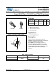
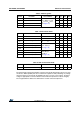
3 Test circuits
Figure 14. Switching times test circuit for
resistive load
Figure 15. Gate charge test circuit
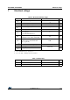
Figure 16. Test circuit for inductive load
switching and diode recovery times
Figure 17. Unclamped inductive load test circuit
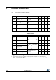
Figure 18. Unclamped inductive waveform Figure 19. Switching time waveform
AM01468v1
VGS
PW
VD
RG
RL
D.U.T.
2200
μF
3.3
μF
V
DD
AM01469v1
VDD
47kΩ
1kΩ
47kΩ
2.7kΩ
1kΩ
12V
V
i=20V=VGMAX
2200
μF
PW
IG=CONST
100Ω
100nF
D.U.T.
V
G
AM01470v1
A
D
D.U.T.
S
B
G
25
Ω
A
A
B
B
R
G
G
FAST
DIODE
D
S
L=100μH
μF
3.3
1000
μF
V
DD
AM01471v1
Vi
Pw
VD
ID
D.U.T.
L
2200
μF
3.3
μF
VDD
AM01472v1
V(BR)DSS
VDD
VDD
VD
IDM
ID
AM01473v1
VDS
ton
tdon
tdoff
toff
tf
tr
90%
10%
10%
0
0
90%
90%
10%
V
GS