
Datasheet


DocID025377 Rev 1 5/14
STF7N80K5, STFI7N80K5 Electrical characteristics
14
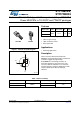
The built-in back-to-back Zener diodes have been specifically designed to enhance not only
the device's ESD capability, but also to make them capable of safely absorbing any voltage
transients that may occasionally be applied from gate to source. In this respect, the Zener
voltage is appropriate to achieve efficient and cost-effective protection of device integrity.
The integrated Zener diodes thus eliminate the need for external components.
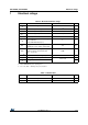
Table 6. Switching times
Symbol Parameter Test conditions Min. Typ. Max. Unit
t
d(on)
Turn-on delay time
V
DD
= 400 V, I
D
= 3 A,
R
G
=4.7 Ω, V
GS
=10 V
(see Figure 17)
-11.3- ns
t
r
Rise time 8.3 ns
t
d(off)
Turn-off delay time 23.7 ns
t
f
Fall time 20.2 ns
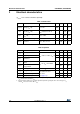
Table 7. Source drain diode
Symbol Parameter Test conditions Min. Typ. Max. Unit
I
SD
Source-drain current - 6 A
I
SDM
Source-drain current (pulsed) - 24 A
V
SD
(1)
1. Pulsed: pulse duration = 300µs, duty cycle 1.5%
Forward on voltage I
SD
= 6 A, V
GS
=0 - 1.5 V
t
rr
Reverse recovery time
I
SD
= 6 A, V
DD
= 60 V
di/dt = 100 A/µs,
(see Figure 16)
- 315 ns
Q
rr
Reverse recovery charge - 2.8 µC
I
RRM
Reverse recovery current - 17.5 A
t
rr
Reverse recovery time I
SD
= 6 A,V
DD
= 60 V
di/dt=100 A/µs,
Tj=150 °C
(see Figure 16)
- 480 ns
Q
rr
Reverse recovery charge - 3.8 µC
I
RRM
Reverse recovery current - 16 A
Table 8. Gate-source Zener diode
Symbol Parameter Test conditions Min Typ. Max Unit
V
(BR)GSO
Gate-source breakdown voltage I
GS
= ± 1mA, I
D
=0 30 - - V