
Datasheet
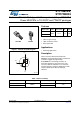


Electrical characteristics STF7N80K5, STFI7N80K5
4/14 DocID025377 Rev 1
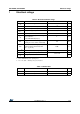
2 Electrical characteristics
(T
CASE
= 25 °C unless otherwise specified).
Table 4. On/off states
Symbol Parameter Test conditions Min. Typ. Max. Unit
V
(BR)DSS
Drain-source breakdown
voltage (V
GS
= 0)
I
D
= 1 mA 800 V
I
DSS
Zero gate voltage drain
current (V
GS
= 0)
V
DS
= 800 V
V
DS
= 800 V, Tc=125 °C
1
50
µA
µA
I
GSS
Gate body leakage current
(V
DS
= 0)
V
GS
= ± 20 V ±10 µA
V
GS(th)
Gate threshold voltage V
DS
= V
GS
, I
D
= 100 µA 3 4 5 V
R
DS(on)
Static drain-source on-
resistance
V
GS
= 10 V, I
D
= 3 A 0.95 1.2 Ω
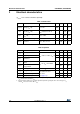
Table 5. Dynamic
Symbol Parameter Test conditions Min. Typ. Max. Unit
C
iss
Input capacitance
V
DS
=100 V, f=1 MHz, V
GS
=0
-360- pF
C
oss
Output capacitance - 30 - pF
C
rss
Reverse transfer
capacitance
-1-pF
C
o(tr)
(1)
1. Time related is defined as a constant equivalent capacitance giving the same charging time as C
oss
when
V
DS
increases from 0 to 80% V
DSS
Equivalent capacitance time
related
V
GS
= 0, V
DS
= 0 to 640 V
-47-pF
C
o(er)
(2)
2. Energy related is defined as a constant equivalent capacitance giving the same stored energy as C
oss
when V
DS
increases from 0 to 80% V
DSS
Equivalent capacitance
energy related
-20-pF
R
G
Intrinsic gate resistance f = 1 MHz, I
D
=0 - 6 - Ω
Q
g
Total gate charge
V
DD
= 640 V, I
D
= 6 A
V
GS
=10 V
(see Figure 15)
- 13.4 - nC
Q
gs
Gate-source charge - 3.7 - nC
Q
gd
Gate-drain charge - 7.5 - nC