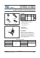
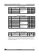
STD4N80K5, STF4N80K5, STP4N80K5, STU4N80K5 N-channel 800 V, 2.1 Ω typ., 3 A MDmesh™ K5 Power MOSFETs in DPAK, TO-220FP, TO-220 and IPAK packages Datasheet - production data Features TAB Order code VDS RDS(on) max. ID PTOT 3 STD4N80K5 1 DPAK 60 W 3 1 STF4N80K5 2 800 V TO-220FP TAB 20 W 2.5 Ω 3A STP4N80K5 60 W STU4N80K5 TAB 1 2 3 3 2 1 IPAK TO-220 • Industry’s lowest RDS(on) x area • Industry’s best figure of merit (FoM) • Ultra low gate charge • 100% avalanche tested Figure 1.
Contents STD4N80K5, STF4N80K5, STP4N80K5, STU4N80K5 Contents 1 Electrical ratings . . . . . . . . . . . . . . . . . . . . . . . . . . . . . . . . . . . . . . . . . . . . 3 2 Electrical characteristics . . . . . . . . . . . . . . . . . . . . . . . . . . . . . . . . . . . . . 4 2.1 Electrical characteristics (curves) . . . . . . . . . . . . . . . . . . . . . . . . . . . . . . . . 6 3 Test circuits .............................................. 9 4 Package information . . . . . . . . . . . . . . . .
STD4N80K5, STF4N80K5, STP4N80K5, STU4N80K5 1 Electrical ratings Electrical ratings Table 2. Absolute maximum ratings Value Symbol Parameter DPAK, IPAK Unit TO-220FP TO-220 VDS Drain-source voltage 800 V VGS Gate- source voltage ±30 V ID Drain current (continuous) at TC = 25 °C 3 ID Drain current (continuous) at TC = 100 °C 1.7 Drain current (pulsed) 12 Total dissipation at TC = 25 °C 60 IDM (2) PTOT 3 (1) 3 A 1.7 (1) 1.
Electrical characteristics 2 STD4N80K5, STF4N80K5, STP4N80K5, STU4N80K5 Electrical characteristics (Tcase =25 °C unless otherwise specified) Table 4. On /off states Symbol V(BR)DSS Parameter Test conditions Drain-source breakdown voltage ID = 1 mA, VGS = 0 IDSS VDS = 800 V Zero gate voltage drain current (VGS = 0) VDS = 800 V, TC=125 °C IGSS Gate-body leakage current (VDS = 0) Min. Typ. Gate threshold voltage VDS = VGS, ID = 100 µA RDS(on) Static drain-source onVGS = 10 V, ID = 1.
STD4N80K5, STF4N80K5, STP4N80K5, STU4N80K5 Electrical characteristics Table 6. Switching times Symbol td(on) tr Parameter Test conditions Turn-on delay time VDD = 400 V, ID = 1.5 A, RG = 4.7 Ω, VGS = 10 V (see Figure 18) Rise time td(off) tf Turn-off-delay time Fall time Min. Typ. Max. Unit - 16.5 - ns - 15 - ns - 36 - ns - 21 - ns Table 7. Source drain diode Symbol ISD ISDM (1) VSD (2) Parameter Test conditions Source-drain current Min. Typ. Max.
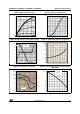
Electrical characteristics 2.1 STD4N80K5, STF4N80K5, STP4N80K5, STU4N80K5 Electrical characteristics (curves) Figure 2. Safe operating area for DPAK and IPAK Figure 3. Thermal impedance for DPAK and IPAK AM15986v1 ID (A) Tj=150°C Tc=25°C Single pulse 10 Op Lim era ite tion d by in t m his ax ar RD ea S( on is 10µs 100µs ) 1 1ms 10ms 0.1 0.01 0.1 10 1 100 VDS(V) Figure 4. Safe operating area for TO-220FP Figure 5.
STD4N80K5, STF4N80K5, STP4N80K5, STU4N80K5 Figure 8. Output characteristics Electrical characteristics Figure 9. Transfer characteristics AM15989v1 ID (A) AM15990v1 ID (A) VGS=10, 11 V 5 VDS=20V 5 9V 4 4 3 3 8V 2 2 7V 1 1 6V 0 4 0 12 8 16 0 VDS(V) Figure 10. Gate charge vs gate-source voltage AM15991v1 VDS (V) VGS (V) VDD=640V ID=3A VDS 12 600 10 500 8 400 6 300 4 200 2 100 7 6 5 8 9 10 VGS(V) Figure 11.
Electrical characteristics STD4N80K5, STF4N80K5, STP4N80K5, STU4N80K5 Figure 14. Normalized on-resistance vs temperature AM15640v1 RDS(on) (norm) VGS=10V ID=1.5 A 2.4 Figure 15. Source-drain diode forward characteristics AM15994v1 VSD (V) 1 2 0.9 1.6 0.8 1.2 0.7 0.8 0.6 TJ=-50°C TJ=25°C TJ=150°C 0.4 -50 0.5 0 50 100 0.5 TJ(°C) Figure 16. Normalized VDS vs temperature 1 2 1.5 2.5 Figure 17. Maximum avalanche energy vs.
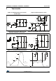
STD4N80K5, STF4N80K5, STP4N80K5, STU4N80K5 3 Test circuits Test circuits Figure 18. Switching times test circuit for resistive load Figure 19. Gate charge test circuit VDD 12V 47kΩ 1kΩ 100nF 3.3 μF 2200 RL μF IG=CONST VDD VGS 100Ω Vi=20V=VGMAX VD RG 2200 μF D.U.T. D.U.T. VG 2.7kΩ PW 47kΩ 1kΩ PW AM01468v1 Figure 20. Test circuit for inductive load switching and diode recovery times A A AM01469v1 Figure 21. Unclamped inductive load test circuit L A D G D.U.T.
Package information 4 STD4N80K5, STF4N80K5, STP4N80K5, STU4N80K5 Package information In order to meet environmental requirements, ST offers these devices in different grades of ECOPACK® packages, depending on their level of environmental compliance. ECOPACK® specifications, grade definitions and product status are available at: www.st.com. ECOPACK® is an ST trademark.
STD4N80K5, STF4N80K5, STP4N80K5, STU4N80K5 4.1 Package information DPAK(TO-252), package information Figure 24.
Package information STD4N80K5, STF4N80K5, STP4N80K5, STU4N80K5 Figure 25. DPAK (TO-252) mechanical data mm Dim. Min. Typ. A 2.20 2.40 A1 0.90 1.10 A2 0.03 0.23 b 0.64 0.90 b4 5.20 5.40 c 0.45 0.60 c2 0.48 0.60 D 6.00 6.20 D1 E 5.10 6.40 6.60 E1 4.70 e 2.28 e1 4.40 4.60 H 9.35 10.10 L 1.00 1.50 L1 2.80 L2 0.80 L4 0.60 1.00 R V2 12/23 Max. 0.
STD4N80K5, STF4N80K5, STP4N80K5, STU4N80K5 Package information Figure 26. DPAK (TO-252) footprint (a) )3 B5 a.
Package information 4.2 STD4N80K5, STF4N80K5, STP4N80K5, STU4N80K5 TO-220FP, package information Figure 27.
STD4N80K5, STF4N80K5, STP4N80K5, STU4N80K5 Package information Table 9. TO-220FP mechanical data mm Dim. Min. Typ. Max. A 4.4 4.6 B 2.5 2.7 D 2.5 2.75 E 0.45 0.7 F 0.75 1 F1 1.15 1.70 F2 1.15 1.70 G 4.95 5.2 G1 2.4 2.7 H 10 10.4 L2 16 L3 28.6 30.6 L4 9.8 10.6 L5 2.9 3.6 L6 15.9 16.4 L7 9 9.3 Dia 3 3.
Package information 4.3 STD4N80K5, STF4N80K5, STP4N80K5, STU4N80K5 TO-220, package information Figure 28.
STD4N80K5, STF4N80K5, STP4N80K5, STU4N80K5 Package information Table 10. TO-220 type A mechanical data mm Dim. Min. Typ. Max. A 4.40 4.60 b 0.61 0.88 b1 1.14 1.70 c 0.48 0.70 D 15.25 15.75 D1 1.27 E 10 10.40 e 2.40 2.70 e1 4.95 5.15 F 1.23 1.32 H1 6.20 6.60 J1 2.40 2.72 L 13 14 L1 3.50 3.93 L20 16.40 L30 28.90 ∅P 3.75 3.85 Q 2.65 2.
Package information 4.4 STD4N80K5, STF4N80K5, STP4N80K5, STU4N80K5 IPAK(TO-251), package information Figure 29.
STD4N80K5, STF4N80K5, STP4N80K5, STU4N80K5 Package information Table 11. IPAK (TO-251) type A mechanical data mm. DIM min. typ. max. A 2.20 2.40 A1 0.90 1.10 b 0.64 0.90 b2 b4 0.95 5.20 B5 5.40 0.30 c 0.45 0.60 c2 0.48 0.60 D 6.00 6.20 E 6.40 6.60 e e1 2.28 4.40 H 4.60 16.10 L 9.00 9.40 L1 0.80 1.20 L2 0.80 V1 10° DocID025105 Rev 3 1.
Packaging mechanical data 5 STD4N80K5, STF4N80K5, STP4N80K5, STU4N80K5 Packaging mechanical data Table 12. DPAK (TO-252) tape and reel mechanical data Tape Reel mm mm Dim. Dim. Min. Max. A0 6.8 7 A B0 10.4 10.6 B 1.5 12.1 C 12.8 1.6 D 20.2 G 16.4 50 B1 20/23 Min. Max. 330 13.2 D 1.5 D1 1.5 E 1.65 1.85 N F 7.4 7.6 T K0 2.55 2.75 P0 3.9 4.1 Base qty. 2500 P1 7.9 8.1 Bulk qty. 2500 P2 1.9 2.1 R 40 T 0.25 0.35 W 15.7 16.3 DocID025105 Rev 3 18.
STD4N80K5, STF4N80K5, STP4N80K5, STU4N80K5 Packaging mechanical data Figure 30. Tape for DPAK (TO-252) 10 pitches cumulative tolerance on tape +/- 0.2 mm T P0 Top cover tape P2 D E F B1 W K0 B0 For machine ref. only including draft and radii concentric around B0 A0 P1 D1 User direction of feed R Bending radius User direction of feed AM08852v1 Figure 31. Reel for DPAK (TO-252) T REEL DIMENSIONS 40mm min.
Revision history 6 STD4N80K5, STF4N80K5, STP4N80K5, STU4N80K5 Revision history Table 13. Document revision history Date Revision 09-Aug-2013 1 First release 13-Dec-2013 2 – Added: IPAK package – Added: Table 11 and Figure 29 – Minor text changes 3 – Updated title and description in cover page. – Updated Table 2.: Absolute maximum ratings, Table 5.: Dynamic and Table 7.: Source drain diode. – Updated 4: Package information and 5: Packaging mechanical data. – Minor text changes.
STD4N80K5, STF4N80K5, STP4N80K5, STU4N80K5 IMPORTANT NOTICE – PLEASE READ CAREFULLY STMicroelectronics NV and its subsidiaries (“ST”) reserve the right to make changes, corrections, enhancements, modifications, and improvements to ST products and/or to this document at any time without notice. Purchasers should obtain the latest relevant information on ST products before placing orders. ST products are sold pursuant to ST’s terms and conditions of sale in place at the time of order acknowledgement.