
Datasheet
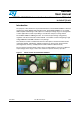

UM0984 Board description
Doc ID 17812 Rev 2 9/25
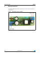
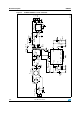
3.2 Description of main components
The complete converter application consists of an input section and the flyback converter
itself.
3.2.1 The input section contains
Bridge diode rectifier (DB1)
The bridge diode rectifier is used to reduce the size of the input bulk capacitor.
Inrush current limiter (R1)
This component reduces the inrush current caused by the connection of the SMPS to
the mains (charging current of bulk capacitors) or by surge pulses. It is recommended
to use a wirewound resistor to get higher immunity against current spikes.
EMI filter (L1, C1, C2, C13)
This basic EMI pi-filter uses an X2 foil capacitor (C1), bulk capacitors (C2, C13) and
a CMC inductor (L1).
Input bulk capacitors (C2, C13)
These capacitors store energy when the input AC voltage is low. Their value respects
the minimum input voltage and output power. The maximum voltage of these capacitors
is 450 V for this design because the maximum input voltage is specified up to 305 VAC.
If the maximum input voltage of the application is lower (more often the value is 265
VAC), 400 V capacitors can be used.
3.2.2 The flyback converter consists of
VIPER26LD (IC1)
This device integrates a controller and high voltage power MOSFET in one package.
The controller works in current mode with a fixed frequency and in discontinuous mode
even at the lowest input voltage. Thanks to the built-in error amplifier, the VIPER26LD
can directly sense the auxiliary voltage via a voltage divider (R5, R6). Thanks to good
coupling of the auxiliary and secondary windings, the auxiliary voltage corresponds
well with the secondary voltage and can be used for feedback regulation. Mandatory
components for proper operation of the VIPer26 are V
DD
capacitor C4 and
compensation network R8, C6 and C7. Diode D2 provides auxiliary voltage to C4 and
the feedback voltage divider.
Note: The voltage divider collecting feedback information for the FB pin is connected to the V
DD
pin. The total resistance of this voltage divider has to be designed with respect to the
minimum charging current during startup and additional possible leakage currents (V
DD
capacitor). The minimum charging current is 600 µA, the maximum leakage current through
the V
DD
capacitor can be theoretically in the range of several tens of µA. The total current
through the voltage divider is therefore set to 150 µA to guarantee enough margin for the
startup circuit.