
Datasheet


UM0984 Board description
Doc ID 17812 Rev 2 11/25
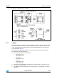
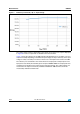
Figure 4. Transformer construction
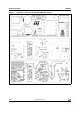
3.4 Layout
The layout of the PCB is based on a single-sided FR4, with 35 µm thickness. The size of the
PCB is 32 x 90 mm. The distance between the primary and secondary side is higher than
8 mm, respecting the safety requirements for all standard applications. The layout of the
PCB is provided in Figure 5.
The layout was designed with respect to the following rules to achieve stable operation,
good efficiency and reduce EMI noise.
● The power HF tracks are wide and short:
– Transformer to IC1
– Transformer to C13
– IC1 to C13
– Transformer to C8
– C8 to D3
– Transformer to D3
– Peak clamp loop
● The power and signal GND of VIPER26LD are separated and connected only in one
point close to the source pins
● The EMI filter has been placed far from the transformer to avoid possible crosstalk of
EMI noise