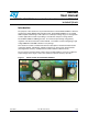
UM0984 User manual STEVAL-ISA081V1 demonstration board based on a 12 V / 1 A isolated flyback Introduction The purpose of this document is to provide information on the STEVAL-ISA081V1 switched mode power supply (SMPS) demonstration board. The STEVAL-ISA081V1 is an isolated SMPS capable of delivering a 12 W output over a wide input voltage range. It is designed for a mains application focused on providing a cost-effective and space saving solution.
Contents UM0984 Contents 1 Main characteristics . . . . . . . . . . . . . . . . . . . . . . . . . . . . . . . . . . . . . . . . . 5 2 Board connection . . . . . . . . . . . . . . . . . . . . . . . . . . . . . . . . . . . . . . . . . . . 6 3 Board description . . . . . . . . . . . . . . . . . . . . . . . . . . . . . . . . . . . . . . . . . . . 7 4 5 6 2/25 3.1 Schematic . . . . . . . . . . . . . . . . . . . . . . . . . . . . . . . . . . . . . . . . . . . . . . . . . . 7 3.
Document alternate name List of tables List of tables Table 1. Table 2. Table 3. Table 4. Table 5. Transformer windings . . . . . . . . . . . . . . . . . . . . . . . . . . . . . . . . . . . . . . . . . . . . . . . . . Bill of materials . . . . . . . . . . . . . . . . . . . . . . . . . . . . . . . . . . . . . . . . . . . . . . . . . . . . . . Settings and performance of demonstration board for different output voltages . . . . Efficiency using a 60 V Schottky diode . . . . . . . . . . . . . . . . . . . .
List of figures UM0984 List of figures Figure 1. Figure 2. Figure 3. Figure 4. Figure 5. Figure 6. Figure 7. Figure 8. Figure 9. Figure 10. Figure 11. Figure 12. Figure 13. Figure 14. 4/25 Demonstration board STEVAL-ISA081V1 . . . . . . . . . . . . . . . . . . . . . . . . . . . . . . . . . Input/output connection of SMPS . . . . . . . . . . . . . . . . . . . . . . . . . . . . . . . . . . . . . . . . STEVAL-ISA081V1 circuit schematic . . . . . . . . . . . . . . . . . . . . . . . . . . . . . . . . . . . .
UM0984 1 Main characteristics Main characteristics The main characteristics of the SMPS are listed below ● ● Input: – VIN: 85 ~ 305 Vrms – frequency: 45 ~ 66 Hz Output: – 12 VDC ± 10%, 1 A (at 3.3 V not loaded) – 3.
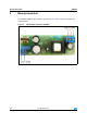
Board connection 2 UM0984 Board connection The STEVAL-ISA081V1 demonstration board is shown in Figure 2 below, with input and output locations. Figure 2.
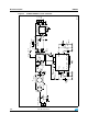
UM0984 Board description 3 Board description 3.1 Schematic A schematic diagram of the isolated flyback converter board prototype based on the VIPER26LD is provided in Figure 3 on page 8.
/25 * # N& 8 2 n Doc ID 17812 Rev 2 6 6 2 $ 344( 2 ! 2 2 P& 6 # # 6 N& # 2 2 . ! &" 6$$ . # '.$ '.$ ,)- #/-0 )# $ 6IPER ,$ . $2!). $2!). $2!). $2!). 6 # # 2 OPT 6 N& # N& # 2 N& 6 # $ 3403 ( # P& # OPT 2 . ! 42 %& N& 9 ' ' ' ' # N& )# , , !# 6 ).
UM0984 3.2 Board description Description of main components The complete converter application consists of an input section and the flyback converter itself. 3.2.1 The input section contains Bridge diode rectifier (DB1) The bridge diode rectifier is used to reduce the size of the input bulk capacitor. Inrush current limiter (R1) This component reduces the inrush current caused by the connection of the SMPS to the mains (charging current of bulk capacitors) or by surge pulses.
Board description UM0984 Peak clamp (D1, R2, R3, C3) This circuit absorbs energy from the voltage spike present after MOSFET turn-off. This spike is generated by leakage inductance of the transformer. Alternatively, a Transil™based peak clamp can be used - for instance PKC-136. The application of this device allows reducing standby consumption and it can also save some space on the board. Secondary side (D3, C8, C11, R9, C9, IC2, C10) The main secondary part is a rectifier consisting of D3 and C8.
UM0984 Board description Figure 4. 3.4 Transformer construction Layout The layout of the PCB is based on a single-sided FR4, with 35 µm thickness. The size of the PCB is 32 x 90 mm. The distance between the primary and secondary side is higher than 8 mm, respecting the safety requirements for all standard applications. The layout of the PCB is provided in Figure 5. The layout was designed with respect to the following rules to achieve stable operation, good efficiency and reduce EMI noise.
Board description Figure 5.
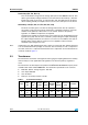
UM0984 Board description 3.5 BOM Table 2. Bill of materials Index Quantity Ref. Value / generic part number 1 1 R1 5.1 Ω / 2 W Wirewound 4.7 Ω / 2 W Wirewound 51 kΩ / 5% / 0.25 W 1206 or Package / class 2 2 R2, R3 3 1 R4 3.9 Ω / 5% / 0.1 W 0805 4 1 R5 150 kΩ /1% / 0.1 W 0805 5 1 R6 43 kΩ / 1% / 0.1 W 0805 6 0 R7 Not assembled 7 1 R8 10 kΩ / 5% / 0.1 W 8 0 R9 Not assembled 9 1 C1 100 nF / 305 VAC / X2 18 x 5 x 11 RM 15 10 1 C2 10 µF / 450 V D12.
Board description Table 2. UM0984 Bill of materials (continued) Index Quantity Ref. 32 1 J1 Screw terminal 2 pos. RM 5 mm 33 1 J2 Screw terminal 3 pos.
UM0984 Measurements 4 Measurements 4.1 Efficiency Figure 6. Efficiency at 120 VAC and 230 VAC vs.
Measurements Figure 7. UM0984 Efficiency at full load (1 A) vs. input voltage The output voltage efficiency depending on the output current of the 12 V output is displayed in Figure 6. The 3.3 V output was not loaded for this measurement. Figure 7 shows the efficiency of the SMPS at full load applied on the 12 V output (1 A, 3.3 V output not loaded) depending on the different input voltages.
UM0984 Measurements 4.2 Standby Figure 8. Standby power vs. input voltage The standby behavior of the board is displayed in Figure 8. The blue line is the standby input power of the fully assembled board. The red line is the standby input power of the board without linear regulator L78L33 and with a 15 V Zener diode applied as a bleeder. The typical input current of L78L33 is 3.5 mA which is approximately 40 mW of load present on the secondary side.
Measurements 4.3 Load regulation Figure 9. 12 V output load regulation UM0984 The load regulation of the 12 V output is displayed in Figure 9. The output voltage at no output load is determined by the consumption of L78L33. If L78L33 is not implemented and no other bleeder (Zener diode or resistor) is used, the output voltage rises. The load regulation of the 3.3 V output is visible in Figure 10.
UM0984 Measurements Figure 10. 3.3 V output load regulation The output voltage of the 3.3 V and 12 V output at no load depending on the input voltage is visible in Figure 11. Figure 11. Output voltage at no load vs.
Measurements 4.4 UM0984 EMI The conductive EMI test of the demonstration board is displayed in Figure 12. The AVG detector is indicated on the left, the peak detector measurement is indicated on the right. Figure 12.
UM0984 4.5 Measurements Temperature The thermal map at full load, measured at 305 VAC and at 85 VAC, is displayed in Figure 13 and Figure 14. The ambient temperature was 25 °C. Figure 13. Thermal map of the board at 305 V AC on the input - left bottom side, right top side Figure 14.
Application recommendations UM0984 5 Application recommendations 5.1 Output voltage operating range The demonstration board STEVAL-ISA081V1 was originally designed for output specification 12 V / 1 A supplied from wide input range 85 to 305 VAC. With minimal changes of components it is possible to set a different output voltage in the nominal output voltage range of 10 to 18 V, keeping the output power capability. The only changes are in the values of voltage divider R5, R6.
UM0984 5.2 Application recommendations Improved efficiency The measured efficiency is about 84% at full output load and 230 VAC. This value can be increased by simply changing the output Schottky diode. Please note that the original board contains an STPS3H100 - 3 A / 100 V Schottky diode. This diode is universal - applicable also up to 18 V output voltage. If only 12 V output is required, a 60 V Schottky diode can be used. An STPS5L60 - 5 A / 60 V Schottky diode in the SMC package was tested.
Revision history 6 UM0984 Revision history Table 5. 24/25 Document revision history Date Revision Changes 25-Nov-2010 1 Initial release. 08-Jun-2012 2 Updated Figure 3, minor text corrections throughout document.
UM0984 Please Read Carefully: Information in this document is provided solely in connection with ST products. STMicroelectronics NV and its subsidiaries (“ST”) reserve the right to make changes, corrections, modifications or improvements, to this document, and the products and services described herein at any time, without notice. All ST products are sold pursuant to ST’s terms and conditions of sale.