
User manual


TSM1052 Electrical characteristics
5/15
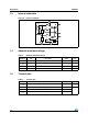
2 Electrical characteristics
T
J
= 25 °C and V
CC
= 5 V, unless otherwise specified
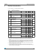
Table 5. Electrical characteristics
Symbol Parameter Test conditions Min Typ Max Unit
Device supply
V
CC
Voltage operating range 1.7 18 V
I
CC
Quiescent current
(Ictrl = Vsense = Vctr = 0,
OUT = open)
150
µA
(1)
1. Specification referred to -10 °C < T
A
< 85 °C
300
Voltage control loop op amp
Gm
v
Transconductance
(sink current only)
(2)
2. If the voltage on Vctrl (the negative input of the amplifier) is higher than the positive amplifier input
(Vref = 1.21 V), and it is increased by 1mV, the sinking current at the output OUT will be increased by
3.5 mA.
13.5
S
(1)
2.5
Vref Voltage reference
(3)
3. The internal Voltage Reference is set at 1.21 V (bandgap reference). The voltage control loop precision
takes into account the cumulative effects of the internal voltage reference deviation as well as the input
offset voltage of the transconductance operational amplifier. The internal Voltage Reference is fixed by
bandgap, and trimmed to 0.5% accuracy at room temperature.
1.198 1.21 1.222
V
(1)
1.186 1.234
Ibias Inverting input bias current
50
nA
(1)
100
Current control loop
Gm
i
Transconductance
(sink current only)
(4)
4. When the positive input at Ictrl is lower than -200 mV, and the voltage is decreased by 1mV, the sinking
current at the output Out will be increased by 7 mA.
1.5 7
S
(1)
Vsense
Current loop reference
(5)
@ I(Iout) = 1 mA
5. The internal current sense threshold is set at -200 mV. The current control loop precision takes into
account the cumulative effects of the internal voltage reference deviation as well as the input offset voltage
of the transconductance operational amplifier.
196 200 204
mV
(1)
192 208
Ibias
Non-inverting input source current @
V(Ictrl) = -200 mV
20
µA
(1)
40
Output stage
V
OUTlow
Low output level @ 2 mA sink current
100
mV
(1)
200