
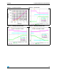
Datasheet
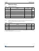

Pin configuration STCS2A
4/18
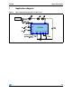
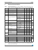
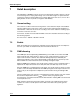
2 Pin configuration
Figure 2. Pin connections (top view)
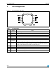
Table 2. Pin description
Pin n° Symbol Note
1V
CC
Supply voltage
2 PWM PWM dimming input
3ENShutdown
4 NC No connect
5 DRAIN Internal N-MOSFET drain
6 SOURCE
Internal N-MOSFET source. Reference voltage is 100 mV. An external resistor between
SOURCE and GND pins sets different current levels for different application needs
7FB
Feedback input. The control loop regulates the current in such a way that the average
voltage at the FB input is 100 mV (nominal). The cathode of the LED and a resistor to
ground to set the LED current should be connected at this point
8 GND Ground
9 SLOPE Capacitor for slope control
10 DISC Load disconnection flag (open drain)
exp-pad Internally connected to ground