
Datasheet
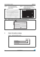

Order information scheme SMLVT3V3
4/7 Doc ID 4146 Rev 4
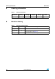
Figure 8. Relative variation of leakage current versus junction temperature
2 Order information scheme
Figure 9. Ordering information scheme
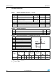
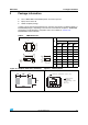
Figure 6. Peak forward voltage drop
versus peak forward current
(typical values)
Figure 7. Transient thermal impedance,
junction to ambient, versus pulse
duration (PCB - FR4)
0.01
0.10
1.00
1.0E-03 1.0E-02 1.0E-01 1.0E+00 1.0E+01 1.0E+02 1.0E+03
Z
th(j-a)
/R
th(j-a)
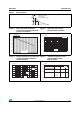
Recommended pad layout
t
P
(µs)
SM LVT 3V3
Surface Mount
Low voltage Transil
Stand off voltage
3V3 = 3.3 V