
Datasheet

SMLVT3V3 Characteristics
Doc ID 4146 Rev 4 3/7
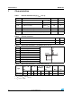
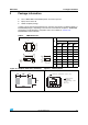
Figure 1. Pulse waveform
Repetitive pulse current
t
r
= rise time (µs)
t
p
= pulse duration time (µs)
t
r
t
p
Figure 2. Peak pulse power dissipation
versus initial junction temperature
(printed circuit board)
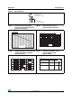
Figure 3. Peak pulse power versus
exponential pulse duration
0 25 50 75 100 125 150 175 200
0.0
0.1
0.2
0.3
0.4
0.5
0.6
0.7
0.8
0.9
1.0
1.1
Tj initial (°C)
P [Tj initial]
PP
P [Tj initial = 25° C]PP
0.1
1.0
10.0
100.0
1.0E-03 1.0E-02 1.0E-01 1.0E+00 1.0E+01
P
PP
(kW)
T
j
initial = 25 °C
t
P
(ms)
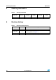
Figure 4. Clamping voltage versus peak pulse
current (exponential waveform,
maximum values)
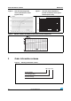
Figure 5. Junction capacitance versus
reverse applied voltage
(typical values)
0.1 1.0 10.0 100.0
4
6
8
10
V
CL(V)
Ipp(A)
tp=1ms
tp=20 µs
12345
1000
2000
3000
4000
5000
V
R(V)
C(pF)
F=1MHz
Tj=25°C