
User manual


Device registers VL6180X
40/79 DocID026171 Rev 6
6 Device registers
This section describes in detail all user accessible device registers. Registers are grouped
by function as shown in Table 22. to make them easier to read but also to simplify multi-byte
read/write I
2
C accesses (burst mode). More details in Section 5. Reset values are given for
each register which denotes the register value in software standby.
Note that registers can be 8-,16- or 32-bit. Multi-byte registers are always addressed in
ascending order with MSB first as shown in Table 23.
6.1 Register encoding formats
Some registers are encoded to allow rational numbers to be expressed efficiently. Table 24
gives an explanation of 9.7 and 4.4 encoding formats.
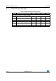
Table 22. Register groups
Register group Address range
IDENTIFICATION 0x00 - 0x0F
SYSTEM SETUP 0x10 - 0x17
RANGE SETUP 0x18 - 0x37
ALS SETUP 0x38 - 0x40
RESULTS 0x4D - 0x80
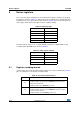
Table 23. 32-bit register example
Register address Byte
Address MSB
Address + 1 ..
Address + 2 ..
Address + 3 LSB
Table 24. 9.7 and 4.4 register formats
Format Description
4.4
8 bits = 4 integer bits + 4 fractional bits (stored as 1 byte)
Encoding example: the value 4.2 is multiplied by 16 (2
4
) rounded
and stored as 67 decimal.
Decoding example: 67 is divided by 16 = 4.19.
9.7
16 bits = 9 integer bits + 7 fractional bits (stored over 2 bytes)
Encoding example: the value 4.2 is multiplied by 128 (2
7
) rounded
and stored as 537 decimal.
Decoding example: 537 is divided by 128 = 4.19.