
User manual


Functional description VL6180X
14/79 DocID026171 Rev 6
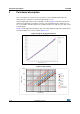
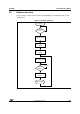
2.2 Timing diagram
Figure 9 and Table 4.show the Root part number 1 power-up timing constraints.
• AVDD_VCSEL must be applied before or at the same time as AVDD.
• GPIO0 defaults to an active low shutdown input. When GPIO0 = 0, the device is in
hardware standby. If GPIO0 is not used it should be connected to AVDD.
• The internal microprocessor (MCU) boot sequence commences when AVDD is up and
GPIO0 is high whichever is the later.
• GPIO1 power-up default is output low. It is tri-stated during the MCU boot sequence.
Note: In hardware standby, GPIO1 is output low and will sink current through any pull-up resistor.
This leakage can be minimized by increasing the value of the pull-up resistor.
• After the MCU boot sequence the device enters software standby. The software
standby state can be determined by polling
SYSTEM__FRESH_OUT_OF_RESET{0x16}. Host initialization can commence
immediately after entering software standby.
Figure 9. Power-up timing
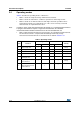
Table 4. Power-up timing constraints
Symbol Parameter Min Max Unit
t1 AVDD_VCSEL power applied after AVDD - 0 ms
t2 Minimum reset on GPIO0 100 - ns
t3 GPIO1 output low after hardware standby - 400 μs
t4 MCU boot - 1 ms
t5 Software standby to host initialization - 0 ms
AVDD
AVDD_VCSEL
GPIO0 (optional)
GPIO1
System state
fresh_out_of_reset
hardware
standby
hardware
standby
software
standby
mcu boot
software
standby
t1
t2
t3
t5
t4
I
2
C Comms
t3
mcu boot