
User manual


DocID026171 Rev 6 11/79
VL6180X Overview
78
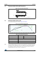
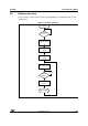
1.5 Recommended solder pad dimensions
Figure 4. Recommended solder pattern
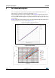
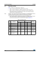
1.6 Recommended reflow profile
The recommend reflow profile is shown in Figure 5 and Table 3.
Figure 5. Recommended reflow profile
Note: As the VL6180X package is not sealed, only a dry re-flow process should be used (such as
convection re-flow). Vapor phase re-flow is not suitable for this type of optical component.
The VL6180X is an optical component and as such, it should be treated carefully. This
would typically include using a ‘no-wash’ assembly process.
0.55 mm
0.60 mm
Pad pitch 0.75 mm
1.40 mm
Same as device pad dimensions
Table 3. Recommended reflow profile
Profile Ramp to strike
Temperature gradient in preheat (T= 70 - 180°C): 0.9 +/- 0.1°C/s
Temperature gradient (T= 200 - 225°C): 1.1 - 3.0°C/s
Peak temperature in reflow 237°C - 245°C
Time above 220°C 50 +/- 10 seconds
Temperature gradient in cooling -1 to -4 °C/s (-6°C/s maximum)
Time from 50 to 220°C 160 to 220 seconds