
User manual


Overview VL6180X
10/79 DocID026171 Rev 6
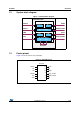
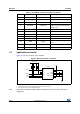
1.4 Application schematic
Figure 3 shows the schematic of the VL6180X.
Figure 3. Root part number 1 schematic
1. Open drain. Recommend 47 kΩ
2. Open drain. Pull up resistors typically fitted once per I
2
C bus at host
3. No connects can also be grounded if required
Note: Capacitors on AVDD and AVDD_VCSEL should be placed as close as possible to the
supply pads.
Table 2. VL6180X pin numbers and signal descriptions
Pin number Signal name Signal type Signal description
1 GPIO1 Digital I/O Interrupt output. Open-drain.
2 NC No connect or ground
3 NC No connect or ground
4 GPIO0/CE Digital I/O
Power-up default is chip enable
(CE). It should be pulled high with a
47 kΩ resistor.
5 SCL Digital input I
2
C serial clock
6 SDA Digital I/O I
2
C serial data
7 NC No connect or ground
8 AVDD_VCSEL Supply VCSEL power supply. 2.6 to 3.0 V
9 AVSS_VCSEL Ground VCSEL ground
10 AVDD Supply
Digital/analog power supply. 2.6 to
3.0 V
11 NC No connect or ground
12 AVSS Ground Digital/analog ground
VL6180X
1
6
7
12
GPIO1
NC
NC
(3)
SCL
SDA
GPIO0
AVSS
AVDD
NC
AVDD_VCSEL
NC
AVSS_VCSEL
3
4
5
8
9
10
112
2.8V
1.8V or 2.8V
GPIO1
(1)
GPIO0
(1)
SCL
(2)
SDA
(2)
4.7 uF
100 nF