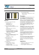
VL6180X Proximity and ambient light sensing (ALS) module Datasheet - production data • Two programmable GPIO – Window and thresholding functions for both ranging and ALS Description Features • Three-in-one smart optical module – Proximity sensor – Ambient Light Sensor – VCSEL light source • Fast, accurate distance ranging – Measures absolute range from 0 to above 10 cm – Independent of object reflectance – Ambient rejection – Crosstalk compensation for cover glass – Ranging beyond 100mm is possible with
Contents VL6180X Contents 1 2 Overview . . . . . . . . . . . . . . . . . . . . . . . . . . . . . . . . . . . . . . . . . . . . . . . . . . 8 1.1 Technical specification . . . . . . . . . . . . . . . . . . . . . . . . . . . . . . . . . . . . . . . . 8 1.2 System block diagram . . . . . . . . . . . . . . . . . . . . . . . . . . . . . . . . . . . . . . . . 9 1.3 Device pinout . . . . . . . . . . . . . . . . . . . . . . . . . . . . . . . . . . . . . . . . . . . . . . . 9 1.4 Application schematic . .
VL6180X Contents 2.13 3 4 2.12.2 Cross-talk . . . . . . . . . . . . . . . . . . . . . . . . . . . . . . . . . . . . . . . . . . . . . . . . 27 2.12.3 Offset calibration procedure . . . . . . . . . . . . . . . . . . . . . . . . . . . . . . . . . . 27 2.12.4 Cross-talk calibration procedure . . . . . . . . . . . . . . . . . . . . . . . . . . . . . . 28 2.12.5 Cross-talk limit . . . . . . . . . . . . . . . . . . . . . . . . . . . . . . . . . . . . . . . . . . . . 29 2.12.6 Cross-talk vs air gap .
Contents 4/79 VL6180X 6.2.8 IDENTIFICATION__TIME . . . . . . . . . . . . . . . . . . . . . . . . . . . . . . . . . . . 45 6.2.9 SYSTEM__MODE_GPIO0 . . . . . . . . . . . . . . . . . . . . . . . . . . . . . . . . . . 46 6.2.10 SYSTEM__MODE_GPIO1 . . . . . . . . . . . . . . . . . . . . . . . . . . . . . . . . . . 47 6.2.11 SYSTEM__HISTORY_CTRL . . . . . . . . . . . . . . . . . . . . . . . . . . . . . . . . . 48 6.2.12 SYSTEM__INTERRUPT_CONFIG_GPIO . . . . . . . . . . . . . . . . . . . . . . 49 6.2.
VL6180X Contents 6.2.45 RESULT__RANGE_REFERENCE_RATE . . . . . . . . . . . . . . . . . . . . . . . 65 6.2.46 RESULT__RANGE_RETURN_SIGNAL_COUNT . . . . . . . . . . . . . . . . . 65 6.2.47 RESULT__RANGE_REFERENCE_SIGNAL_COUNT . . . . . . . . . . . . . 66 6.2.48 RESULT__RANGE_RETURN_AMB_COUNT . . . . . . . . . . . . . . . . . . . . 66 6.2.49 RESULT__RANGE_REFERENCE_AMB_COUNT . . . . . . . . . . . . . . . . 66 6.2.50 RESULT__RANGE_RETURN_CONV_TIME . . . . . . . . . . . . . . . . . . . . 67 6.2.
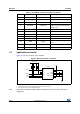
List of tables VL6180X List of tables Table 1. Table 2. Table 3. Table 4. Table 5. Table 6. Table 7. Table 8. Table 9. Table 10. Table 11. Table 12. Table 13. Table 14. Table 15. Table 16. Table 17. Table 18. Table 19. Table 20. Table 21. Table 22. Table 23. Table 24. Table 25. Table 26. Table 27. Table 28. 6/79 Technical specification . . . . . . . . . . . . . . . . . . . . . . . . . . . . . . . . . . . . . . . . . . . . . . . . . . . . . 8 VL6180X pin numbers and signal descriptions. . . . . . . . . .
VL6180X List of figures List of figures Figure 1. Figure 2. Figure 3. Figure 4. Figure 5. Figure 6. Figure 7. Figure 8. Figure 9. Figure 10. Figure 11. Figure 12. Figure 13. Figure 14. Figure 15. Figure 16. Figure 17. Figure 18. Figure 19. Figure 20. Figure 21. Figure 22. Figure 23. Figure 24. Figure 25. Figure 26. Figure 27. Figure 28. Figure 29. Figure 30. Figure 31. Figure 32. VL6180X block diagram . . . . . . . . . . . . . . . . . . . . . . . . . . . . . . . . . . . . . . . . . . . . . . . . . . . .
Overview 1 VL6180X Overview This datasheet is applicable to the final VL6180X ROM code revision. 1.1 Technical specification Table 1. Technical specification Feature Detail Package Optical LGA12 Size 4.8 x 2.8 x 1.0 mm Ranging 0 to 100 mm(1) Ambient light sensor < 1 Lux up to 100 kLux(2) 16-bit output(3) 8 manual gain settings Operating voltage: • Functional range • Optimum range(4) 2.6 to 3.0 V 2.7 to 2.
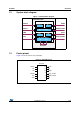
VL6180X 1.2 Overview System block diagram Figure 1. VL6180X block diagram VL6180X module VL6180X silicon GPIO-0 Ranging GPIO-1 Microcontroller SDA NVM SCL AVDD ALS AVDD_VCSEL RAM IR emitter driver IR- AVSS AVSS_VCSEL IR+ IR emitter 1.3 Device pinout Figure 2 shows the pinout of the VL6180X. Figure 2.
Overview VL6180X Table 2. VL6180X pin numbers and signal descriptions 1.4 Pin number Signal name Signal type Signal description 1 GPIO1 Digital I/O 2 NC No connect or ground 3 NC No connect or ground 4 GPIO0/CE Digital I/O 5 SCL Digital input I2C serial clock 6 SDA Digital I/O I2C serial data 7 NC 8 AVDD_VCSEL Supply VCSEL power supply. 2.6 to 3.0 V 9 AVSS_VCSEL Ground VCSEL ground 10 AVDD Supply Digital/analog power supply. 2.6 to 3.
VL6180X 1.5 Overview Recommended solder pad dimensions Figure 4. Recommended solder pattern Pad pitch 0.75 mm 1.40 mm 0.60 mm 0.55 mm 1.6 Same as device pad dimensions Recommended reflow profile The recommend reflow profile is shown in Figure 5 and Table 3. Figure 5. Recommended reflow profile Table 3. Recommended reflow profile Profile Note: Ramp to strike Temperature gradient in preheat (T= 70 - 180°C): 0.9 +/- 0.1°C/s Temperature gradient (T= 200 - 225°C): 1.1 - 3.
Functional description 2 VL6180X Functional description This section gives an overview of the key features of the VL6180X and describes the different modes of operation of the ALS and proximity sensors. Typical ranging performance of the VL6180X is shown in Figure 6. This demonstrates the reflectance independence and range accuracy of the VL6180X from 0 to 100 mm for 3%, 5%, 17% and 88% reflective targets. The example shown here is with ST cover glass and a 1.0 mm air gap.
VL6180X 2.1 Functional description System state diagram Figure 8 describes the main operating states of the VL6180X. Hardware standby is the reset state (GPIO0=0)(a). The device is held in reset until GPIO0 is de-asserted. Note that the device will not respond to I2C communication in this mode. When GPIO0=1, the device enters software standby after the internal MCU boot sequence has completed.
Functional description 2.2 VL6180X Timing diagram Figure 9 and Table 4.show the Root part number 1 power-up timing constraints. Note: • AVDD_VCSEL must be applied before or at the same time as AVDD. • GPIO0 defaults to an active low shutdown input. When GPIO0 = 0, the device is in hardware standby. If GPIO0 is not used it should be connected to AVDD. • The internal microprocessor (MCU) boot sequence commences when AVDD is up and GPIO0 is high whichever is the later.
VL6180X 2.3 Functional description Software overview Figure 10 shows a simple start-up routine from initialization to completing a range or ALS measurement. Figure 10.
Functional description 2.4 VL6180X Operating modes Table 5. describes the operating modes of this device. Note: • Modes 1 and 2 are single-shot range and ALS measurements. • Modes 3 and 4 are stand-alone, continuous operation for either range or ALS. • Modes 5 and 6 are for mixed continuous and single-shot mode operations where regular measurements are required from one of the sensors and only occasional measurements are required from the other.
VL6180X 2.4.1 Functional description Single-shot range/ALS operation A single-shot range or ALS measurement is performed as follows: • Write 0x01 to the SYSRANGE__START register{0x18}. • When the measurement is completed, bit 2 of RESULT__INTERRUPT_STATUS_GPIO{0x4F} will be set. • Similarly, a single-shot ALS measurement is initiated by writing 0x01 to the SYSALS__START register{0x38}. • When the measurement is completed, bit 5 of RESULT__INTERRUPT_STATUS_GPIO{0x4F} will be set.
Functional description 2.4.3 VL6180X Interleaved mode Figure 11. describes the continuous interleaved mode of operation where an ALS measurement is immediately followed by a range measurement and repeated after an interval specified by the ALS inter-measurement period. To enable interleaved mode, set INTERLEAVED_MODE_ENABLE{0x2A3} = 1. Use SYSALS__START and SYSALS__INTERMEASUREMENT_PERIOD to control interleaved operation. Note: Continuous range settings have no effect in this mode. Figure 11.
VL6180X Functional description Table 6. Interleaved mode limits (10 Hz operation) Parameter 2.5 Period (ms) SYSALS__INTERMEASUREMENT_PERIOD 100 Effective ALS INTERMEASUREMENT PERIOD 90 SYSRANGE__MAX_CONVERGENCE_TIME 30 Total RANGE EXECUTION TIME 35 SYSALS__INTEGRATION_TIME 50 Total ALS INTEGRATION TIME 55 TOTAL EXECUTION TIME 90 Range timing Figure 12 gives a breakdown of total execution time for a single range measurement. Note: • The pre-calibration phase is fixed (3.2 ms).
Functional description VL6180X Table 7. Typical range convergence time (ms) Target reflectance Range (mm) 2.6 3% 5% 17% 88% 10 0.43 0.33 0.18 0.18 20 0.94 0.73 0.28 0.18 30 1.89 1.40 0.51 0.18 40 3.07 2.25 0.81 0.18 50 4.35 3.24 1.18 0.24 60 5.70 4.22 1.60 0.32 70 7.07 5.35 2.07 0.49 80 8.41 6.45 2.58 0.50 90 9.58 7.56 3.14 0.61 100 10.73 8.65 3.69 0.
VL6180X Functional description Table 8. Range error codes Bits [7:4] 0 Error code Description Range (mm) 0 - 200(1) No error Valid measurement System error System error detected. No measurement possible. 255 6 Early convergence estimate ECE check failed 255 7 Max convergence System did not converge before the specified max. convergence time limit 255 8 Range ignore Ignore threshold check failed 255 Not used - 11 SNR Ambient conditions too high.
Functional description VL6180X return signal rate 0.5 ms after the start of every measurement. If it is below the ECE threshold, the measurement is aborted and an ECE error is flagged. Figure 13. Early convergence estimate (ECE) Return count convergence threshold converged m in n ur et .r si g l na ra ECE threshold te measurement aborted ECE (0.5 ms) time max. convergence ECE is enabled by setting bit 0 of SYSRANGE__RANGE_CHECK_ENABLES{0x02D}.
VL6180X 2.8.3 Functional description Signal-to-noise ratio (SNR) In high ambient conditions range accuracy can be impaired so the SNR threshold is used as a safety limit to invalidate range measurements where the ambient/signal ratio is considered too high.The default ambient/signal ratio limit is 10 (i.e. an SNR of 0.1) which is then encoded in 4.4 format as follows: SYSRANGE__MAX_AMBIENT_LEVEL_MULT{0x2C}= 10 x 16 = 160 To enable the SNR check, set bit 4 in SYSRANGE__RANGE_CHECK_ENABLES (0x02D).
Functional description VL6180X The buffer is read via eight 16-bit registers (RESULT__HISTORY_BUFFER_0{0x52} to RESULT__HISTORY_BUFFER_7{0x60}). The buffer holds the last 16 x 8-bit range or 8 x 16-bit ALS results as shown in Table 9. Table 9.
VL6180X Functional description the current consumption scales accordingly i.e. the average current consumption at 1 Hz under the same conditions would be 0.17 mA. Figure 14. Typical ranging current consumption (10 Hz sampling rate) ƵƌƌĞŶƚ ĐŽŶƐƵŵƉƚŝŽŶ ;ŵ Ϳ ϰ͘ϱϬ ϰ͘ϬϬ ϯ͘ϱϬ ϯ͘ϬϬ Ϯ͘ϱϬ ϯй Ϯ͘ϬϬ ϱй ϭ͘ϱϬ ϭϳй ϭ͘ϬϬ ϴϴй Ϭ͘ϱϬ Ϭ͘ϬϬ Ϭ ϭϬ ϮϬ ϯϬ ϰϬ ϱϬ ϲϬ ϳϬ ϴϬ ϵϬ ϭϬϬ ZĂŶŐĞ ;ŵŵͿ The minimum average current consumption in Figure 14. is 1.5 mA, 0.
Functional description 2.11.3 VL6180X Current distribution Table 12. shows how current consumption is distributed between the two supplies in ranging mode. AVDD_VCSEL supplies the VCSEL current and AVDD supplies all other functions. Note: The VCSEL driver is pulsed at 100 MHz with a 33% duty cycle (see Figure 15.) so average current consumption on AVDD_VCSEL is one third of the peak. Table 12.
VL6180X 2.12 Functional description Other system considerations This section describes part-to-part range offset and system cross-talk. In addition, a procedure for cross-talk calibration is given. 2.12.1 Part-to-part range offset The VL6180X is factory calibrated to produce an absolute linear range output as shown in Figure 16. The part-to-part range offset is calibrated during manufacture and stored in SYSRANGE__PART_TO_PART_RANGE_OFFSET{0x24} (two’s complement).
Functional description VL6180X 1. Position a white target (88% reflectance(g)) at a distance of 50 mm from the top of the cover glass. 2. Perform a minimum of 10 range measurements and compute the average range (from RESULT__RANGE_VAL{0x62}). 3. If the average range is within the 50 ± 3 mm, offset calibration is not required. Otherwise, complete this calibration procedure. 4. Set SYSRANGE__PART_TO_PART_RANGE_OFFSET{0x24} = 0. 5.
VL6180X 2.12.5 Functional description Cross-talk limit A practical limit for cross-talk is < 3.0 Mcps. This is based on two factors: The return rate for a 3% reflective target at 100 mm without glass is typically around 1.5 Mcps. If glass is added with a cross-talk of 3.0 Mcps, the resultant return rate will be 4.5 Mcps. This results in a cross-talk correction factor of x3 so for a 100 mm target the raw range will be in the region of 30 mm.
Functional description 2.13 VL6180X Ambient light sensor (ALS) The VL6180X contains an ambient light sensor capable of measuring the ambient light level over a wide dynamic range. This section describes the main features of the ALS. The ALS performance specification can be found in Section 4.2. 2.13.1 Field of view Figure 19 shows the ALS field of view which is typically 42 degrees (half angle, 40% of peak) in both X and Y. Figure 19.
VL6180X 2.13.3 Functional description ALS dynamic range Table 13 shows the range of measurable light at all gains both with and without glass. In most applications operating at a single gain setting should be possible. Table 13. ALS dynamic range(1) Analogue gain setting Dynamic range (no glass) Dynamic range (10% transmissive glass) Min. (Lux)(2) Max. (Lux) 1 3.20 20800 32.0 >100,000 1.25 2.56 16640 25.6 >100,000 1.67 1.93 12530 19.3 >100,000 2.5 1.28 8320 12.8 83,200 5 0.
Functional description 2.13.5 VL6180X Integration period The integration period is the time over which a single ALS measurement is made. The default integration period is 100ms. Integration times in the range 50-100 ms are recommended to reduce impact of light flicker from artificial lighting. 2.13.6 ALS gain selection Eight analog gain settings are available which can be selected manually depending on the range and resolution required. Table 14.
VL6180X Electrical characteristics 3 Electrical characteristics 3.1 Absolute maximum ratings Table 15. Absolute maximum ratings Parameter Min. Typ. Max. Unit AVDD -0.5 - 3.6 V AVDD_VCSEL -0.5 - 3.6 V SCL, SDA, GPIO0 and GPIO1 -0.5 - 3.6 V Note: Stresses above those listed in Table 15. may cause permanent damage to the device.
Electrical characteristics 3.4 VL6180X Electrical characteristics Table 18. Digital I/O electrical characteristics Symbol Parameter Minimum Typical Maximum Unit CMOS digital I/O (SDA, SCL, GPIO0 and GPIO1) 34/79 VIL Low level input voltage -0.5 - 0.6 V VIH High level input voltage 1.12 - AVDD+0.5 V VOL Low level output voltage (8mA load) - - 0.4 V VOH High level output voltage (8mA load) AVDD-0.
VL6180X Performance specification 4 Performance specification 4.1 Proximity ranging (0 to 100mm) The following table specifies ranging performance up to 100mm. Ranging beyond 100mm is possible with certain target reflectances and ambient conditions but not guaranteed. These results are derived from characterization of both typical and corner samples (representative of worst case process conditions). Unless specified otherwise, all results were performed at room temperature (23°C), nominal voltage (2.
Performance specification 4.2 VL6180X ALS performance The following table specifies ALS performance. These results are derived from characterization of typical samples (without cover glass). Unless specified otherwise, all tests were performed at room temperature (23°C), nominal voltage (2.8V) and using a halogen light source. Table 21. ALS performance Parameter Min. Typ. Max. Unit 0.28 0.32 0.36 Lux/count - 42 - degrees - photopic - - 0.
I2C control interface VL6180X 5 I2C control interface The VL6180X is controlled over an I2C interface. The default I2C address is 0x29 (7-bit). This section describes the I2C protocol. Figure 21. Serial interface data transfer protocol Acknowledge Start condition SDA MSB SCL S LSB 1 2 3 4 5 P 8 7 6 As/Am Address or data byte Stop condition Information is packed in 8-bit packets (bytes) always followed by an acknowledge bit, As for sensor acknowledge and Am for master acknowledge.
I2C control interface VL6180X As data is received by the slave it is written bit by bit to a serial/parallel register. After each data byte has been received by the slave, an acknowledge is generated, the data is then stored in the internal register addressed by the current index. During a read message, the contents of the register addressed by the current index is read out in the byte following the device address byte.
I2C control interface VL6180X Figure 26.
Device registers 6 VL6180X Device registers This section describes in detail all user accessible device registers. Registers are grouped by function as shown in Table 22. to make them easier to read but also to simplify multi-byte read/write I2C accesses (burst mode). More details in Section 5. Reset values are given for each register which denotes the register value in software standby. Table 22.
VL6180X Device registers Table 25. Register summary Offset Register name Reference 0x000 IDENTIFICATION__MODEL_ID Section 6.2.1 on page 43 0x001 IDENTIFICATION__MODEL_REV_MAJOR Section 6.2.2 on page 43 0x002 IDENTIFICATION__MODEL_REV_MINOR Section 6.2.3 on page 43 0x003 IDENTIFICATION__MODULE_REV_MAJOR Section 6.2.4 on page 44 0x004 IDENTIFICATION__MODULE_REV_MINOR Section 6.2.5 on page 44 0x006 IDENTIFICATION__DATE_HI Section 6.2.
Device registers VL6180X Table 25. Register summary (continued) Offset Register name 0x03E SYSALS__INTERMEASUREMENT_PERIOD Section 6.2.34 on page 58 0x03F SYSALS__ANALOGUE_GAIN Section 6.2.35 on page 59 0x040 SYSALS__INTEGRATION_PERIOD Section 6.2.36 on page 59 0x04D RESULT__RANGE_STATUS Section 6.2.37 on page 60 0x04E RESULT__ALS_STATUS Section 6.2.38 on page 61 0x04F RESULT__INTERRUPT_STATUS_GPIO Section 6.2.39 on page 62 0x050 RESULT__ALS_VAL Section 6.2.
VL6180X Device registers 6.2 Register descriptions 6.2.1 IDENTIFICATION__MODEL_ID 7 6 5 4 3 2 1 0 identification__model_id R/W Address: 0x000 Type: R/W Reset: 0xB4 Description: [7:0] 6.2.2 identification__model_id: Device model identification number. 0xB4 = VL6180X IDENTIFICATION__MODEL_REV_MAJOR 7 6 5 4 3 2 1 RESERVED identification__model_rev_major R R/W Address: 0x001 Type: R/W Reset: 0x1, register default overwritten at boot-up by NVM contents.
Device registers 6.2.4 VL6180X IDENTIFICATION__MODULE_REV_MAJOR 7 6 5 4 3 2 1 RESERVED identification__module_rev_major R R/W Address: 0x003 Type: R/W Reset: 0x1, register default overwritten at boot-up by NVM contents. 0 Description: [2:0] 6.2.5 identification__module_rev_major: Revision identifier of the Module Package for major change. Used to store NVM content version. Contact ST for current information.
VL6180X 6.2.7 Device registers IDENTIFICATION__DATE_LO 7 6 5 4 3 2 1 0 identification__day identification__phase R/W R/W Address: 0x007 Type: R/W Reset: 0xYY, register default overwritten at boot-up by NVM contents. Description: Part of the register set that can be used to uniquely identify a module. [7:3] identification__day: Manufacturing day (bits[4:0]). [2:0] identification__phase: Manufacturing phase identification (bits[2:0]). 6.2.
Device registers 6.2.9 VL6180X SYSTEM__MODE_GPIO0 2 1 0 RESERVED 3 system__gpio0_select 4 system__gpio0_polarity 5 system__gpio0_is_xshutdown 6 RESERVED 7 R R/W R/W R/W R/W Address: 0x010 Type: R/W Reset: 0x60 Description: [6] system__gpio0_is_xshutdown: Priority mode - when enabled, other bits of the register are ignored. GPIO0 is main XSHUTDOWN input. 0: Disabled 1: Enabled - GPIO0 is main XSHUTDOWN input. [5] system__gpio0_polarity: Signal Polarity Selection.
VL6180X 6.2.10 Device registers SYSTEM__MODE_GPIO1 3 2 1 0 RESERVED 4 system__gpio1_select 5 system__gpio1_polarity 6 RESERVED 7 R R/W R/W R/W Address: 0x011 Type: R/W Reset: 0x20 Description: [5] [4:1] [0] system__gpio1_polarity: Signal Polarity Selection. 0: Active-low 1: Active-high system__gpio1_select: Functional configuration options. 0000: OFF (Hi-Z) 1000: GPIO Interrupt output Reserved. Write 0.
Device registers SYSTEM__HISTORY_CTRL Address: 0x012 Type: R/W Reset: 0x0 4 3 2 1 0 system__history_buffer_enable 5 system__history_buffer_mode 6 system__history_buffer_clear 7 RESERVED 6.2.11 VL6180X R R/W R/W R/W Description: 48/79 [2] system__history_buffer_clear: User-command to clear history (FW will auto-clear this bit when clear has completed).
VL6180X 6.2.
Device registers SYSTEM__FRESH_OUT_OF_RESET 6 Address: 0x016 Type: R/W Reset: 0x1 5 4 3 2 1 0 fresh_out_of_reset 7 RESERVED 6.2.14 VL6180X R R/W Description: [0] SYSTEM__GROUPED_PARAMETER_HOLD 6 Address: 0x017 Type: R/W Reset: 0x0 5 4 3 2 1 0 grouped_parameter_hold 7 RESERVED 6.2.
VL6180X SYSRANGE__START Address: 0x018 Type: R/W Reset: 0x0 5 4 3 2 1 0 sysrange__startstop 6 sysrange__mode_select 7 RESERVED 6.2.16 Device registers R R/W R/W Description: [1] sysrange__mode_select: Device Mode select 0: Ranging Mode Single-Shot 1: Ranging Mode Continuous [0] sysrange__startstop: StartStop trigger based on current mode and system configuration of device_ready. FW clears register automatically. Setting this bit to 1 in single-shot mode starts a single measurement.
Device registers 6.2.18 VL6180X SYSRANGE__THRESH_LOW 7 6 5 4 3 2 1 0 sysrange__thresh_low R/W Address: 0x01A Type: R/W Reset: 0x0 Description: [7:0] 6.2.19 sysrange__thresh_low: Low Threshold value for ranging comparison. Range 0-255mm. SYSRANGE__INTERMEASUREMENT_PERIOD 7 6 5 4 3 2 1 0 sysrange__intermeasurement_period R/W Address: 0x01B Type: R/W Reset: 0xFF Description: [7:0] 6.2.
VL6180X 6.2.21 15 Device registers SYSRANGE__CROSSTALK_COMPENSATION_RATE 14 13 12 11 10 9 8 7 6 5 4 3 2 1 0 sysrange__crosstalk_compensation_rate R/W Address: 0x01E Type: R/W Reset: 0x0 Description: [15:0] 6.2.22 sysrange__crosstalk_compensation_rate: User-controlled crosstalk compensation in Mcps (9.7 format). SYSRANGE__CROSSTALK_VALID_HEIGHT 7 6 5 4 3 2 1 0 sysrange__crosstalk_valid_height R/W Address: 0x021 Type: R/W Reset: 0x14 Description: [7:0] 6.2.
Device registers 6.2.24 VL6180X SYSRANGE__PART_TO_PART_RANGE_OFFSET 7 6 5 4 3 2 1 0 1 0 sysrange__part_to_part_range_offset R/W Address: 0x024 Type: R/W Reset: 0xYY, register default overwritten at boot-up by NVM contents. Description: [7:0] 6.2.25 sysrange__part_to_part_range_offset: 2s complement format.
VL6180X 6.2.27 Device registers SYSRANGE__MAX_AMBIENT_LEVEL_MULT 7 6 5 4 3 2 1 0 sysrange__max_ambient_level_mult R/W Address: 0x02C Type: R/W Reset: 0xA0, register default overwritten at boot-up by NVM contents. Description: [7:0] 6.2.28 sysrange__max_ambient_level_mult: User input value to multiply return_signal_count for AMB:signal ratio check. If (amb counts * 6) > return_signal_count * mult then abandon measurement due to high ambient (4.4 format).
Device registers SYSRANGE__VHV_RECALIBRATE Address: 0x02E Type: R/W Reset: 0x0 5 4 3 2 1 0 sysrange__vhv_recalibrate 6 sysrange__vhv_status 7 RESERVED 6.2.29 VL6180X R R/W R/W Description: [1] sysrange__vhv_status: FW controlled status bit showing when FW has completed auto-vhv process. 0: FW has finished autoVHV operation 1: During autoVHV operation [0] sysrange__vhv_recalibrate: User-Controlled enable bit to force FW to carry out recalibration of the VHV setting for sensor array.
VL6180X SYSALS__START 5 Address: 0x038 Type: R/W Reset: 0x0 4 3 2 1 0 sysals__startstop 6 sysals__mode_select 7 RESERVED 6.2.31 Device registers R R/W R/W Description: [1] sysals__mode_select: Device Mode select 0: ALS Mode Single-Shot 1: ALS Mode Continuous [0] sysals__startstop: Start/Stop trigger based on current mode and system configuration of device_ready. FW clears register automatically. Setting this bit to 1 in single-shot mode starts a single measurement.
Device registers 6.2.33 15 VL6180X SYSALS__THRESH_LOW 14 13 12 11 10 9 8 7 6 5 4 3 2 1 0 sysals__thresh_low R/W Address: 0x03C Type: R/W Reset: 0x0 Description: [15:0] 6.2.34 sysals__thresh_low: Low Threshold value for ALS comparison. Range 0-65535 codes.
VL6180X 6.2.35 Device registers SYSALS__ANALOGUE_GAIN 7 6 5 Address: 0x03F Type: R/W Reset: 0x06 4 3 2 1 0 RESERVED sysals__analogue_gain_light R R/W Description: [2:0] 6.2.36 15 sysals__analogue_gain_light: ALS analogue gain (light channel) 0: ALS Gain = 20 1: ALS Gain = 10 2: ALS Gain = 5.0 3: ALS Gain = 2.5 4: ALS Gain = 1.67 5: ALS Gain = 1.25 6: ALS Gain = 1.0 7: ALS Gain = 40 Controls the “light” channel gain. Note: Upper nibble should be set to 0x4 i.e. For ALS gain of 1.
Device registers 3 2 1 0 result__range_max_threshold_hit result__range_measurement_ready result__range_device_ready 7 result__range_min_threshold_hit RESULT__RANGE_STATUS result__range_error_code 6.2.
VL6180X 3 2 1 0 result__als_max_threshold_hit result__als_measurement_ready result__als_device_ready 7 result__als_min_threshold_hit RESULT__ALS_STATUS result__als_error_code 6.2.38 Device registers 6 5 R R R R R Address: 0x04E Type: R Reset: 0x1 4 Description: [7:4] result__als_error_code: Specific error and debug codes 0000: No error 0001: Overflow error 0002: Underflow error [3] result__als_min_threshold_hit: Legacy register - DO NOT USE Use instead 6.2.
Device registers 6.2.
VL6180X 6.2.
Device registers 6.2.42 VL6180X RESULT__RANGE_VAL 7 6 5 4 3 2 1 0 result__range_val R Address: 0x062 Type: R Reset: 0x0 Description: [7:0] 6.2.43 result__range_val: Final range result value presented to the user for use. Unit is in mm. RESULT__RANGE_RAW 7 6 5 4 3 2 1 0 result__range_raw R Address: 0x064 Type: R Reset: 0x0 Description: [7:0] 6.2.44 15 result__range_raw: Raw Range result value with offset applied (no cross talk compensation applied). Unit is in mm.
VL6180X 6.2.45 15 Device registers RESULT__RANGE_REFERENCE_RATE 14 13 12 11 10 9 8 7 6 5 4 3 2 1 0 result__range_reference_rate R Address: 0x068 Type: R Reset: 0x0 Description: [15:0] 6.2.46 result__range_reference_rate: sensor count rate of reference signal returns. Computed from REFERENCE_SIGNAL_COUNT / RETURN_CONV_TIME. Mcps 9.7 format Note: Both arrays converge at the same time, so using the return array convergence time is correct.
Device registers 6.2.47 VL6180X RESULT__RANGE_REFERENCE_SIGNAL_COUNT 31 30 29 28 27 26 25 24 23 22 21 20 19 18 17 16 15 14 13 12 11 10 9 8 7 6 5 4 3 2 1 0 2 1 0 result__range_reference_signal_count R Address: 0x070 Type: R Reset: 0x0 Description: [31:0] 6.2.48 result__range_reference_signal_count: sensor count output value attributed to signal correlated to IR emitter on the Reference array.
VL6180X 6.2.50 Device registers RESULT__RANGE_RETURN_CONV_TIME 31 30 29 28 27 26 25 24 23 22 21 20 19 18 17 16 15 14 13 12 11 10 9 8 7 6 5 4 3 2 1 0 result__range_return_conv_time R Address: 0x07C Type: R Reset: 0x0 Description: [31:0] 6.2.51 result__range_return_conv_time: sensor count output value attributed to signal on the Return array.
Device registers FIRMWARE__BOOTUP 6 5 Address: 0x119 Type: R/W Reset: 0x1 4 3 2 1 0 firmware__bootup 7 RESERVED 6.2.53 VL6180X R R/W Description: [0] 6.2.54 firmware__bootup: FW must set bit once initial boot has been completed. FIRMWARE__RESULT_SCALER 7 6 5 4 3 2 1 RESERVED firmware__als_result_scaler R R/W Address: 0x120 Type: R/W Reset: 0x1 0 Description: [3:0] 6.2.
VL6180X 6.2.56 Device registers INTERLEAVED_MODE__ENABLE 7 6 5 4 3 2 1 0 interleaved_mode__enable R/W Address: 0x2A3 Type: R/W Reset: 0x0 Description: [7:0] Interleaved mode enable: Write 0x1 to this register to select ALS+Range interleaved mode. Use SYSALS__START and SYSALS__INTERMEASUREMENT_PERIOD to control this mode. A range measurement is automatically performed immediately after each ALS measurement.
/79 DocID026171 Rev 6 F E D C B 3267,21 5(7851 $3(5785( $/6 $3(5785( VENT ONLY 2 1 Linear 0 Place Decimals 0 ±0.05 1 Place Decimals 0.0 ±0.05 2 Place Decimals 0.00 ±0.05 Angular ±0.25 degrees Diameter +0.05 0.10 Position Surface Finish 1.
DocID026171 Rev 6 1 Linear 0 Place Decimals 0 ±0.05 1 Place Decimals 0.0 ±0.05 2 Place Decimals 0.00 ±0.05 Angular ±0.25 degrees +0.05 Diameter Position 0.10 Surface Finish 1.
Laser safety considerations 8 VL6180X Laser safety considerations The VL6180X contains a laser emitter and corresponding drive circuitry. The laser output is designed to remain within Class 1 laser safety limits under all reasonably foreseeable conditions including single faults in compliance with IEC 60825-1:2007.
VL6180X 9 Ordering information Ordering information VL6180X is currently available in the following format. More detailed information is available on request. Table 26. Delivery format Order code VL6180XV0NR/1 9.
Ordering information 9.3 VL6180X Packaging The Root part number 1 is available in tape and reel packaging as shown in Figure 31. Figure 31. Tape and reel packaging 4.0 (Po) 1.55+ - 0.1 (Do) 2.0 (P2) B 1.75 (E) 5.5 + - 0.05 (F) 5.10 (Bo) 5° 12.0+ - 0.3 (W) 0.30 + - 0.05 (T) A A B 1.20 (Ko) 8.0 (P1) 1.6 + - 0.05 (D1) SECTION B-B 3.10 (Ao) SECTION A-A Ao + - 0.1 Bo +-0.1 Ko +-0.1 3.10 9.3.1 5.10 1.20 E+ - 0.1 1.75 USER FEED DIRECTION F+ - 0.05 Po +-0.1 P1 +-0.1 P2 +-0.1 Do +-0.
VL6180X 9.4 Ordering information Storage The Root part number 1 is a MSL 3 package. Table 27. Storage conditions Floor Life (out of bag) at Factory Level 3 Ambient <30oC/60% RH 1 Week After this limit, dry bake to be done; 3 hours at 125oC. 9.5 ROHS compliance The Root part number 1 is Ecopack2 compliant as per ST definition.
ECOPACK® 10 VL6180X ECOPACK® In order to meet environmental requirements, ST offers these devices in different grades of ECOPACK® packages, depending on their level of environmental compliance. ECOPACK® specifications, grade definitions and product status are available at: www.st.com. ECOPACK® is an ST trademark.
VL6180X 11 Revision history Revision history Table 28. Document revision history Date Revision 23-Sep-2013 1 Changes Initial release. 1.1 General update for latest ROM revision: Section 1.1: Technical specification updated Section 1.4: Application schematic updated Section 1.5: Recommended solder pad dimensions updated Notes added to Figure 5.: Recommended reflow profile Section 2.13: Ambient light sensor (ALS) updated. Section 3.1: Absolute maximum ratings added Section 3.
Revision history VL6180X Table 28. Document revision history (continued) Date 16-Jun-14 20-Aug-2014 78/79 Revision Changes 5 Re-write of Section 2: Functional description. Section 6: Device registers: Added introduction and minor corrections Section 7: Outline drawing updated to Rev B1. Supplier dependent gate mark added. 6 Updates: Section 2.8.3: Signal-to-noise ratio (SNR): Clarified SNR calculation. Section 6: Device registers: Corrected a clarified some register descriptions.
VL6180X IMPORTANT NOTICE – PLEASE READ CAREFULLY STMicroelectronics NV and its subsidiaries (“ST”) reserve the right to make changes, corrections, enhancements, modifications, and improvements to ST products and/or to this document at any time without notice. Purchasers should obtain the latest relevant information on ST products before placing orders. ST products are sold pursuant to ST’s terms and conditions of sale in place at the time of order acknowledgement.