
Datasheet


Table Of Contents
- Table 1. Device summary
- 1 Package pin connections
- 2 Absolute maximum ratings and operating conditions
- 3 Electrical characteristics
- Table 4. Electrical characteristics at Vcc+ = 2.5 V with Vcc- = 0 V, Vicm = Vcc/2, Tamb = 25° C, and RL connected to Vcc/2 (unless otherwise specified)
- Table 5. Shutdown characteristics VCC = 2.5 V
- Table 6. Electrical characteristics at Vcc+ = 2.7 V with Vcc- = 0 V, Vicm = Vcc/2, Tamb = 25° C, and RL connected to Vcc/2 (unless otherwise specified)
- Table 7. Shutdown characteristics VCC = 2.7 V
- Table 8. Electrical characteristics at Vcc+ = 5 V with Vcc- = 0 V, Vicm = Vcc/2, Tamb = 25° C, and RL connected to Vcc/2 (unless otherwise specified)
- Table 9. Shutdown characteristics VCC = 5 V
- Figure 2. Supply current vs. supply voltage at Vicm = VCC/2
- Figure 3. Supply current vs. Vicm at VCC = 5 V
- Figure 4. Vio distribution at VCC = 5 V
- Figure 5. Input offset voltage vs. input common mode voltage at VCC = 5 V
- Figure 6. Output current vs. output voltage at VCC = 2.7 V
- Figure 7. Output current vs. output voltage at VCC = 5 V
- Figure 8. Output current vs. supply voltage at Vicm = VCC/2
- Figure 9. Voltage gain and phase with CL = 40 pF
- Figure 10. Voltage gain and phase with CL = 100 pF
- Figure 11. Voltage gain and phase with CL = 200 pF
- Figure 12. Phase margin vs. output current at VCC = 5 V
- Figure 13. Stability in follower configuration
- Figure 14. Positive and negative slew rate vs. supply voltage
- Figure 15. Positive slew rate at VCC = 5 V with CL = 100 pF
- Figure 16. Negative slew rate at VCC = 5 V with CL = 100 pF
- Figure 17. Noise vs. frequency at VCC = 5 V
- Figure 18. 0.1 Hz to 10 Hz noise at VCC = 5 V
- Figure 19. Distortion + noise vs. frequency
- Figure 20. Distortion + noise vs. output voltage
- 4 Application information
- 5 Package information
- 5.1 SC70-5 (or SOT323-5) package information
- 5.2 SOT23-5 package information
- 5.3 SOT23-6 package information
- 5.4 DFN8 2 x 2 mm package information
- 5.5 MiniSO-8 package information
- 5.6 MiniSO-10 package information
- 5.7 TSSOP14 package information
- 5.8 TSSOP16 package information
- 5.9 SO-8 package information
- 5.10 SO-14 package information
- 6 Ordering information
- 7 Revision history
Package information LMV82x, LMV82xA
22/32 Doc ID 022467 Rev 3
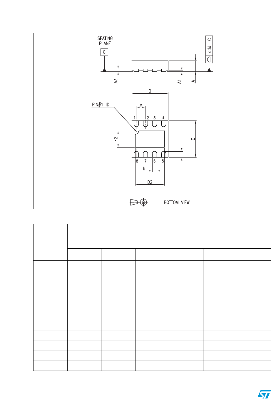
5.4 DFN8 2 x 2 mm package information
Figure 28. DFN8 2 x 2 mm package mechanical drawing (pitch 0.5 mm)
Table 13. DFN8 2 x 2 mm package mechanical data (pitch 0.5 mm)
Ref.
Dimensions
Millimeters Inches
Min. Typ. Max. Min. Typ. Max.
A 0.51 0.55 0.60 0.020 0.022 0.024
A1 0.05 0.002
A3 0.15 0.006
b 0.18 0.25 0.30 0.007 0.010 0.012
D 1.85 2.00 2.15 0.073 0.079 0.085
D2 1.45 1.60 1.70 0.057 0.063 0.067
E 1.85 2.00 2.15 0.073 0.079 0.085
E2 0.75 0.90 1.00 0.030 0.035 0.040
e 0.50 0.020
L0.500.020
ddd 0.08 0.003