
Datasheet


Table Of Contents
- Table 1. Device summary
- 1 Package pin connections
- 2 Absolute maximum ratings and operating conditions
- 3 Electrical characteristics
- Table 4. Electrical characteristics at Vcc+ = 2.5 V with Vcc- = 0 V, Vicm = Vcc/2, Tamb = 25° C, and RL connected to Vcc/2 (unless otherwise specified)
- Table 5. Shutdown characteristics VCC = 2.5 V
- Table 6. Electrical characteristics at Vcc+ = 2.7 V with Vcc- = 0 V, Vicm = Vcc/2, Tamb = 25° C, and RL connected to Vcc/2 (unless otherwise specified)
- Table 7. Shutdown characteristics VCC = 2.7 V
- Table 8. Electrical characteristics at Vcc+ = 5 V with Vcc- = 0 V, Vicm = Vcc/2, Tamb = 25° C, and RL connected to Vcc/2 (unless otherwise specified)
- Table 9. Shutdown characteristics VCC = 5 V
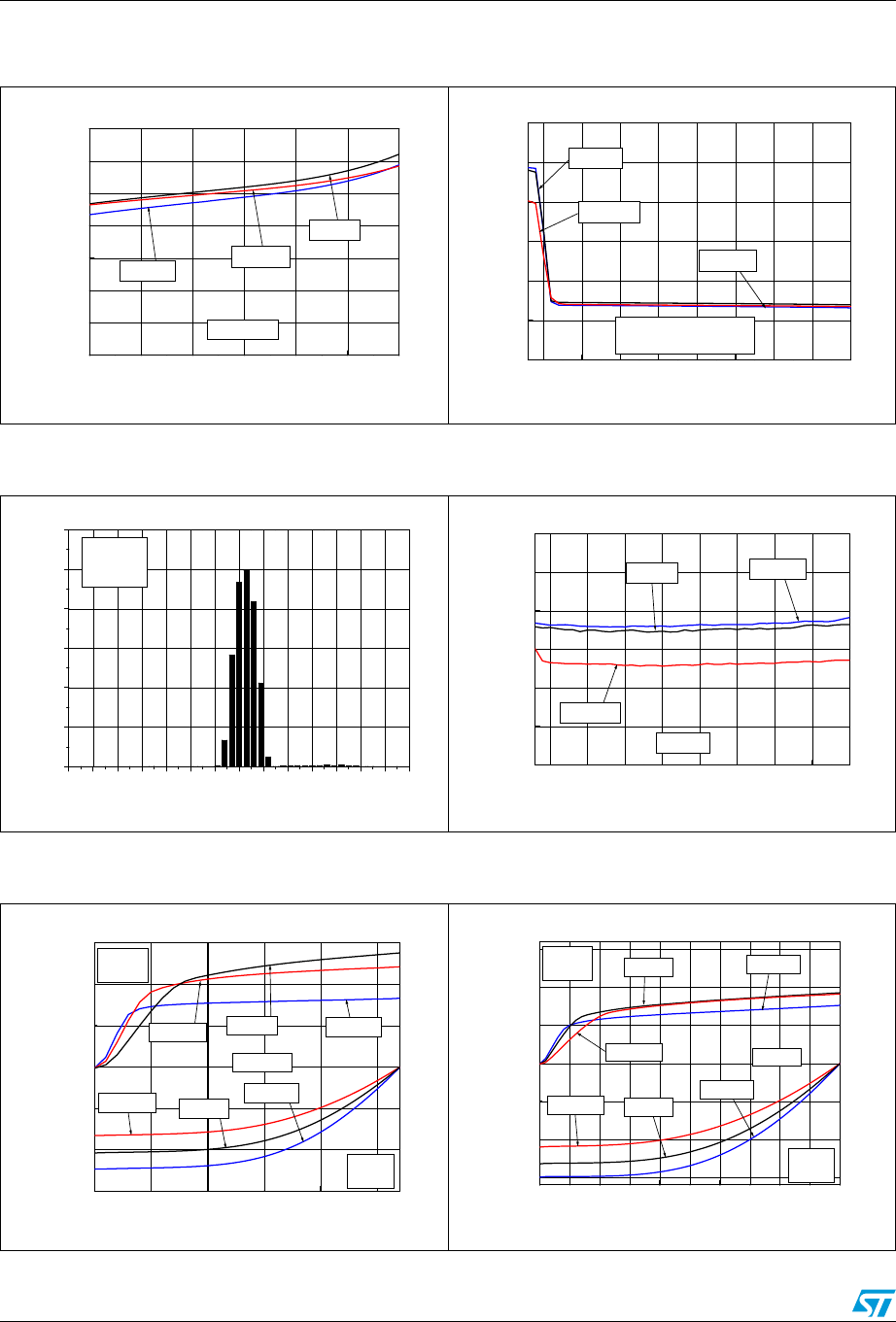
- Figure 2. Supply current vs. supply voltage at Vicm = VCC/2
- Figure 3. Supply current vs. Vicm at VCC = 5 V
- Figure 4. Vio distribution at VCC = 5 V
- Figure 5. Input offset voltage vs. input common mode voltage at VCC = 5 V
- Figure 6. Output current vs. output voltage at VCC = 2.7 V
- Figure 7. Output current vs. output voltage at VCC = 5 V
- Figure 8. Output current vs. supply voltage at Vicm = VCC/2
- Figure 9. Voltage gain and phase with CL = 40 pF
- Figure 10. Voltage gain and phase with CL = 100 pF
- Figure 11. Voltage gain and phase with CL = 200 pF
- Figure 12. Phase margin vs. output current at VCC = 5 V
- Figure 13. Stability in follower configuration
- Figure 14. Positive and negative slew rate vs. supply voltage
- Figure 15. Positive slew rate at VCC = 5 V with CL = 100 pF
- Figure 16. Negative slew rate at VCC = 5 V with CL = 100 pF
- Figure 17. Noise vs. frequency at VCC = 5 V
- Figure 18. 0.1 Hz to 10 Hz noise at VCC = 5 V
- Figure 19. Distortion + noise vs. frequency
- Figure 20. Distortion + noise vs. output voltage
- 4 Application information
- 5 Package information
- 5.1 SC70-5 (or SOT323-5) package information
- 5.2 SOT23-5 package information
- 5.3 SOT23-6 package information
- 5.4 DFN8 2 x 2 mm package information
- 5.5 MiniSO-8 package information
- 5.6 MiniSO-10 package information
- 5.7 TSSOP14 package information
- 5.8 TSSOP16 package information
- 5.9 SO-8 package information
- 5.10 SO-14 package information
- 6 Ordering information
- 7 Revision history
Electrical characteristics LMV82x, LMV82xA
12/32 Doc ID 022467 Rev 3
Figure 2. Supply current vs. supply voltage
at Vicm = V
CC
/2
Figure 3. Supply current vs. Vicm at
V
CC
= 5 V
2.5 3.0 3.5 4.0 4.5 5.0 5.5
0.00
0.05
0.10
0.15
0.20
0.25
0.30
0.35
T=25°C
T=-40°C
T=125°C
Vicm=2.5V
Supply Current (mA)
Supply Voltage (V)
0.0 0.5 1.0 1.5 2.0 2.5 3.0 3.5 4.0
0.0
0.2
0.4
0.6
0.8
1.0
1.2
T=25°C
T=-40°C
T=125°C
Vcc=5V
Follower configuration
Supply Current (mA)
Input Common Mode Voltage (V)
Figure 4. Vio distribution at V
CC
= 5 V Figure 5. Input offset voltage vs. input
common mode voltage at V
CC
= 5 V
-3.5 -3.0 -2.5 -2.0 -1.5 -1.0 -0.5 0.0 0.5 1.0 1.5 2.0 2.5 3.0 3.5
0
5
10
15
20
25
30
Vcc=5V
Vicm=2.5V
T=25°C
Population (%)
Input offset voltage (mV)
0.0 0.5 1.0 1.5 2.0 2.5 3.0 3.5 4.0
0.00
0.05
0.10
0.15
0.20
0.25
0.30
T=25°C
T=-40°C
T=125°C
Vcc=5V
Input Offset Voltage (mV)
Input Common Mode Voltage (V)
Figure 6. Output current vs. output voltage at
V
CC
= 2.7 V
Figure 7. Output current vs. output voltage at
V
CC
= 5 V
0.00.0 0.5 1.01.0 1.5 2.02.0 2.5
-30
-20-20
-10
00
10
2020
30
Source
Vid=1V
Sink
Vid=-1V
T=-40°C
T=25°C
T=125°C
T=-40°C
Vcc=2.7V
T=125°C
T=25°C
Output Current (mA)
Output Voltage (V)
0.00.0 0.5 1.01.0 1.5 2.02.0 2.5 3.03.0 3.5 4.04.0 4.5 5.05.0
-75
-50-50
-25
00
25
5050
75
Source
Vid=1V
Sink
Vid=-1V
T=-40°C
T=25°C
T=125°C
T=-40°C
Vcc=5V
T=125°C
T=25°C
Output Current (mA)
Output Voltage (V)