
Datasheet


Package information LFTVS18-1F3
6/8 Doc ID 14608 Rev 3
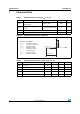
3 Package information
In order to meet environmental requirements, ST offers these devices in different grades of
ECOPACK
®
packages, depending on their level of environmental compliance. ECOPACK
®
specifications, grade definitions and product status are available at: www.st.com.
ECOPACK
®
is an ST trademark.
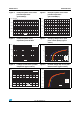
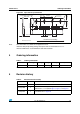
Figure 17. Package dimensions
Note: Product marking may be rotated by 90° for assembly plant differentiation. In no case should
this product marking be used to orient the component for its placement on a PCB. Only pin
1 mark is to be used for this purpose.
Figure 18. Foot print recommendations Figure 19. Marking
185 µm ± 10
185 µm ± 10
0.77 mm ± 30 µm
0.77 mm ± 30 µm
400 µm ± 40
255 µm ± 40
205 µm ± 40
400 µm ± 40
605 µm ± 55
220 µm recommended
220 µm recommended
260 µm maximum
Solder stencil opening:
Copper pad Diameter:
Solder mask opening:
300 µm minimum
x
y
z
w
x
w
Dot,
xx = marking
yww = datecode
y = year,
ww = week
z = manufacturing
location