
Datasheet
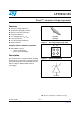
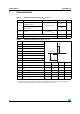
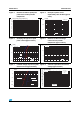
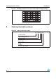
Table Of Contents
- Figure 1. Pin configuration (bump side)
- Figure 2. Device configuration
- 1 Characteristics
- Table 1. Absolute maximum ratings (Tamb = 25 C)
- Table 2. Electrical characteristics (Tamb = 25 C)
- Figure 3. Relative variation of peak pulse power versus initial junction temperature
- Figure 4. Peak pulse power versus exponential pulse duration (typical value)
- Figure 5. Clamping voltage versus peak pulse current (typical values)
- Figure 6. Relative variation of leakage current versus junction temperature (typical values)
- Figure 7. Forward voltage drop versus peak forward current (typical values)
- Figure 8. Junction capacitance versus line voltage (typical values)
- Figure 9. Breakdown voltage versus initial junction temperature (typical value)
- 2 Ordering information scheme
- 3 Package information
- 4 Ordering information
- 5 Revision history
Ordering information LFTVS10-1F3
6/7
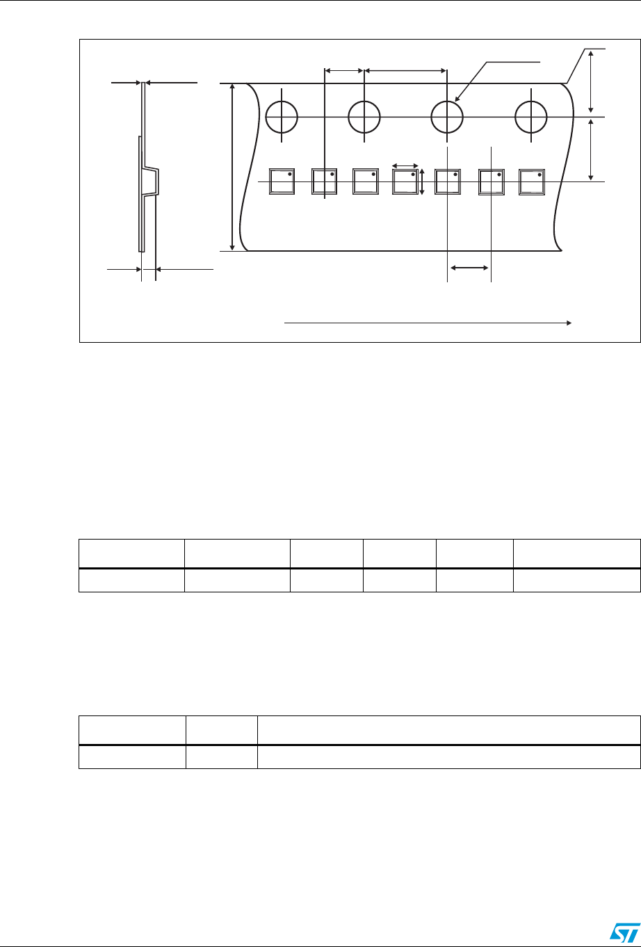
Figure 14. Flip Chip tape and reel specifications
Note: More information is available in the application notes:
AN2348: “400 µm flip chip: Package description and recommendations for use”
AN1751: "EMI Filters: Recommendations and measurements"
4 Ordering information
5 Revision history
User direction of unreeling
All dimensions in mm
4.0 ± 0.1
2.0 ± 0.05
8.0 ± 0.3
2.0 ± 0.1
1.75 ± 0.1 3.5 ±- 0.05
Ø 1.55 ± 0.05
0.69 ± 0.05
0.20 ± 0.05
0.87
0.87
xxz
yww
xxz
yww
xxz
yww
xxz
yww
xxz
yww
xxz
yww
xxz
yww
Table 3. Ordering information
Order code Marking Package Weight Base qty Delivery mode
LFTVS10-1F3 EN Flip Chip 0.86 mg 10 000 Tape and reel (7”)
Table 4. Document revision history
Date Revision Changes
21-Nov-2008 1 Initial release.