
Datasheet
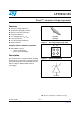
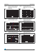
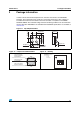
Table Of Contents
- Figure 1. Pin configuration (bump side)
- Figure 2. Device configuration
- 1 Characteristics
- Table 1. Absolute maximum ratings (Tamb = 25 C)
- Table 2. Electrical characteristics (Tamb = 25 C)
- Figure 3. Relative variation of peak pulse power versus initial junction temperature
- Figure 4. Peak pulse power versus exponential pulse duration (typical value)
- Figure 5. Clamping voltage versus peak pulse current (typical values)
- Figure 6. Relative variation of leakage current versus junction temperature (typical values)
- Figure 7. Forward voltage drop versus peak forward current (typical values)
- Figure 8. Junction capacitance versus line voltage (typical values)
- Figure 9. Breakdown voltage versus initial junction temperature (typical value)
- 2 Ordering information scheme
- 3 Package information
- 4 Ordering information
- 5 Revision history
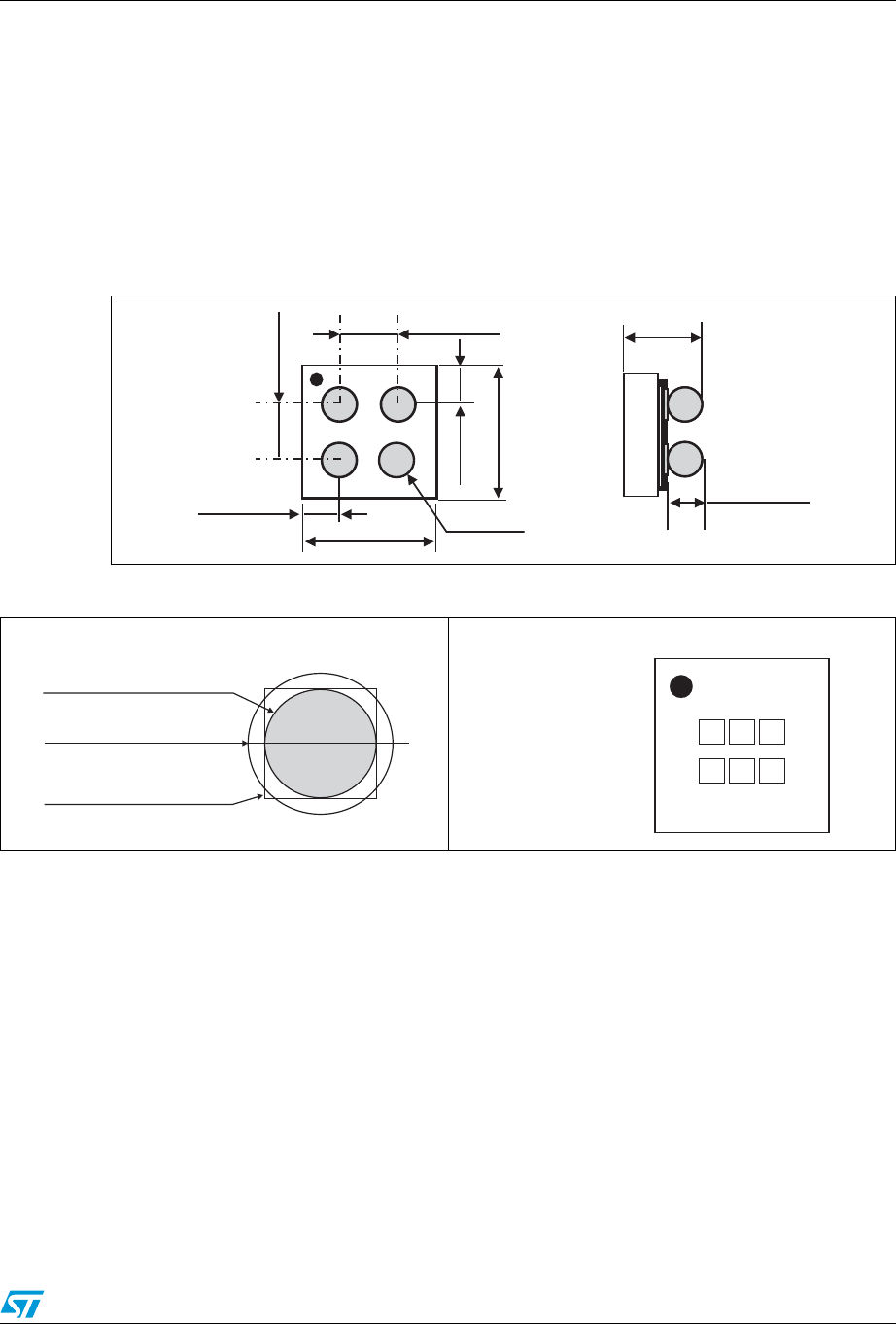
LFTVS10-1F3 Package information
5/7
3 Package information
In order to meet environmental requirements, ST offers these devices in ECOPACK
®
packages. These packages have a lead-free second level interconnect. The category of
second level interconnect is marked on the inner box label, in compliance with JEDEC
Standard JESD97. The maximum ratings related to soldering conditions are also marked on
the inner box label. ECOPACK is an ST trademark. ECOPACK specifications are available at
www.st.com.
Figure 11. Flip Chip dimensions
185 µm ± 10
185 µm ± 10
0.77 mm ± 30 µm
0.77 mm ± 30 µm
400 µm ± 40
255 µm ± 40
205 µm ± 40
400 µm ± 40
605 µm ± 55
Figure 12. Footprint recommendations Figure 13. Marking
220 µm recommended
220 µm recommended
260 µm maximum
Solder stencil opening:
Copper pad Diameter:
Solder mask opening:
300 µm minimum
x
y
x
w
z
w
Dot
xx = marking
yww = datecode
(y = year
ww = week)
z = manufacturing location