
Datasheet
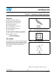
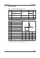
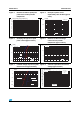
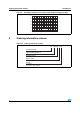
Table Of Contents
- Figure 1. Pin configuration (bump side)
- Figure 2. Device configuration
- 1 Characteristics
- Table 1. Absolute maximum ratings (Tamb = 25 C)
- Table 2. Electrical characteristics (Tamb = 25 C)
- Figure 3. Relative variation of peak pulse power versus initial junction temperature
- Figure 4. Peak pulse power versus exponential pulse duration (typical value)
- Figure 5. Clamping voltage versus peak pulse current (typical values)
- Figure 6. Relative variation of leakage current versus junction temperature (typical values)
- Figure 7. Forward voltage drop versus peak forward current (typical values)
- Figure 8. Junction capacitance versus line voltage (typical values)
- Figure 9. Breakdown voltage versus initial junction temperature (typical value)
- 2 Ordering information scheme
- 3 Package information
- 4 Ordering information
- 5 Revision history
Ordering information scheme LFTVS10-1F3
4/7
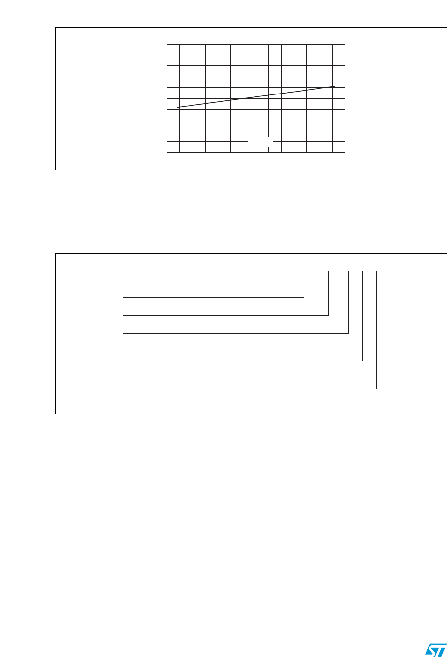
Figure 9. Breakdown voltage versus initial junction temperature (typical value)
2 Ordering information scheme
Figure 10. Ordering information scheme
V (V)
BR
8.0
9.0
10.0
11.0
12.0
13.0
-40 -15 10 35 60 85 110 135
T (° C)
j
LF TVS 10 - 1 F3
Low forward voltage
Transient voltage suppressor
Breakdown voltage
Number of lines
Package
10 = 10 V
MAX
1 = single line
F = Flip Chip
3 = Lead-free, pitch = 400 µm