
Datasheet
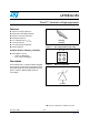
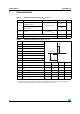
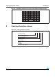
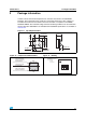
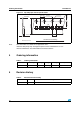
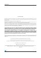
Table Of Contents
- Figure 1. Pin configuration (bump side)
- Figure 2. Device configuration
- 1 Characteristics
- Table 1. Absolute maximum ratings (Tamb = 25 C)
- Table 2. Electrical characteristics (Tamb = 25 C)
- Figure 3. Relative variation of peak pulse power versus initial junction temperature
- Figure 4. Peak pulse power versus exponential pulse duration (typical value)
- Figure 5. Clamping voltage versus peak pulse current (typical values)
- Figure 6. Relative variation of leakage current versus junction temperature (typical values)
- Figure 7. Forward voltage drop versus peak forward current (typical values)
- Figure 8. Junction capacitance versus line voltage (typical values)
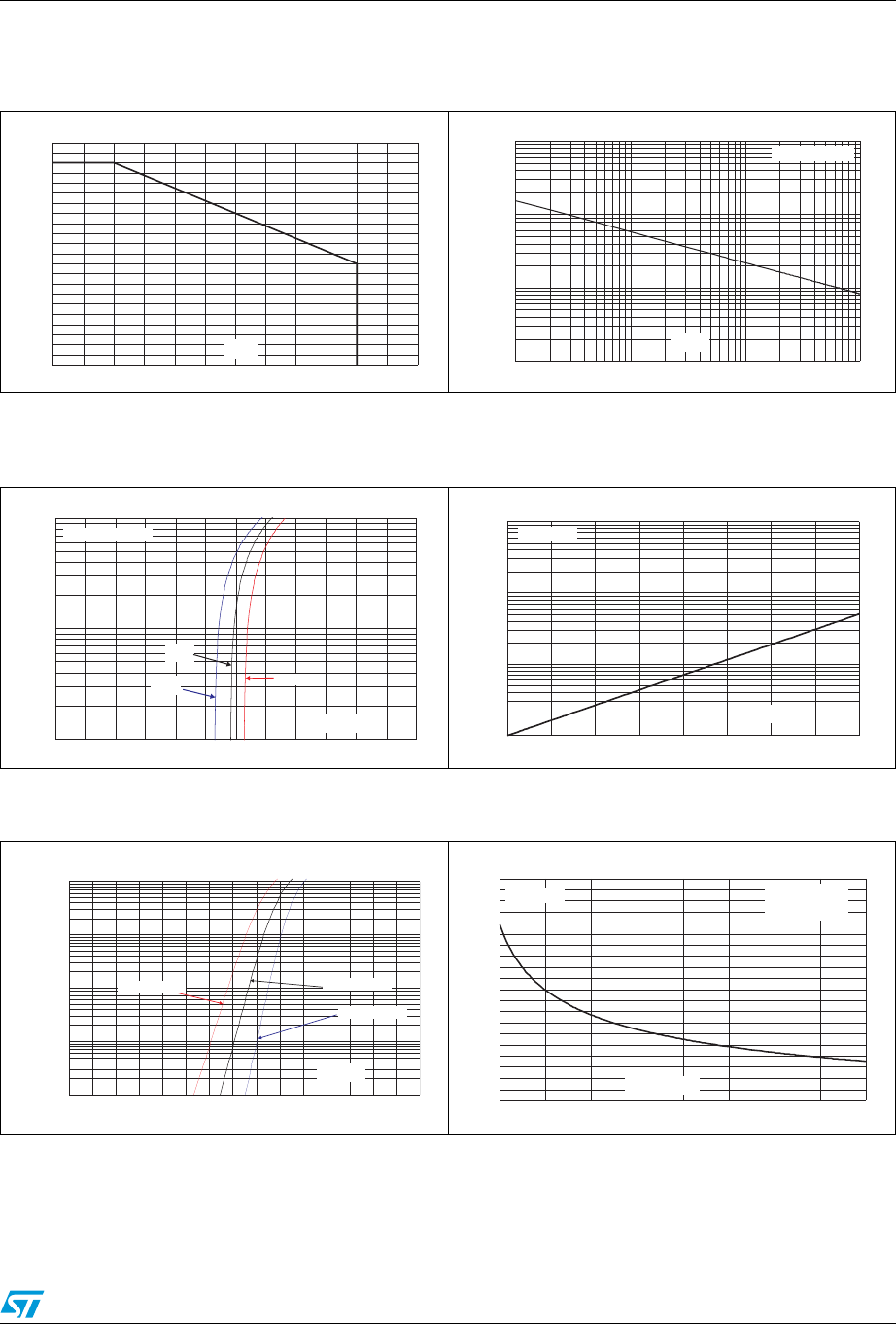
- Figure 9. Breakdown voltage versus initial junction temperature (typical value)
- 2 Ordering information scheme
- 3 Package information
- 4 Ordering information
- 5 Revision history
LFTVS10-1F3 Characteristics
3/7
Figure 3. Relative variation of peak pulse
power versus initial junction
temperature
Figure 4. Peak pulse power versus
exponential pulse duration (typical
value)
0.0
0.1
0.2
0.3
0.4
0.5
0.6
0.7
0.8
0.9
1.0
1.1
0 25 50 75 100 125 150
T (°C)
j
P [T initial] / [T initial=25°C]
PP j j
P
PP
P (W)
PP
10
100
1000
10000
1 10 100 1000
T
j
initial = 25 °C
t (µs)
p
Figure 5. Clamping voltage versus peak
pulse current (typical values)
Figure 6. Relative variation of leakage
current versus junction
temperature (typical values)
Figure 7. Forward voltage drop versus peak
forward current (typical values)
Figure 8. Junction capacitance versus line
voltage (typical values)
0.1
1.0
10.0
5 6 7 8 9 1011121314151617
I (A)
PP
V (V)
CL
-30 °C
25 °C
85 °C
Pulse 8 / 20 µs
I [T ] / I [T =25°C]
Rj Rj
1
10
100
1000
25 50 75 100 125
V
R
=8V
T (°C)
j
0.0001
0.001
0.01
0.1
1
0.0 0.2 0.4 0.6 0.8 1.0 1.2 1.4
I(A)
FM
V(V)
FM
T initial = -30 °C
j
T initial = 25 °C
j
T initial = 85 °C
j
Capacitance(pF)
50
60
70
80
90
100
110
120
130
140
150
160
170
180
190
200
210
220
230
240
250
012345678
F=1 MHz
V
OSC
=30mV
RMS
T
J
=25°C
Vr=0 to 8V
Voltage(V)