
Datasheet


Characteristics LCDP1521
4/12 Doc ID 8627 Rev 4
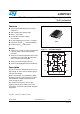
Figure 3. Repetitive peak pulse current
100
50
%I
PP
t
t
t
r
p
0
t
r
: rise time (µs)
t
p
: pulse duration (µs)
ex: Pulse waveform 10/1000 µs
t
r
= 10 µs t
p
= 1000 µs
Table 4. Parameters related to the diode line / GND (T
amb
= 25 °C)
Symbol Test conditions Max Unit
V
F
I
F
= 1 A t = 500 µs 2 V
V
FP
(1)
10/700 µs
1.2/50 µs
2/10 µs
1.5 kV
1.5 kV
2.5 kV
R
S
= 110 Ω
R
S
= 60 Ω
R
S
= 245 Ω
I
PP
= 10 A
I
PP
= 15 A
I
PP
= 10 A
5
10
20
V
1. See Figure 5: Test circuit for V
FP
and V
DGL
parameters. R
S
is the protection resistor located on the line card.
Table 5. Parameters related to the protection thyristor
(T
amb
= 25°C unless otherwise specified)
Symbol Test conditions Min Max Unit
I
GT
V
GND / LINE
= -48 V 0.1 5 mA
I
H
V
GATE
= -48 V
(1)
150 mA
V
GT
At I
GT
2.5 V
I
RG
V
RG
= -150 V
V
RG
= -150 V
T
c
= 25 °C
T
c
= 85 °C
5
50
µA
V
DGL
V
GATE
= -48 V
(2)
10/700 µs
1.2/50 µs
2/10 µs
1.5 kV
1.5 kV
2.5 kV
R
S
= 110 Ω
R
S
= 60 Ω
R
S
= 245 Ω
I
PP
= 10 A
I
PP
= 15 A
I
PP
= 10 A
5
10
20
V
1. See Figure 4: Functional holding current (I
H
) test circuit: go no-go test
2. See Figure 5: Test circuit for V
FP
and V
DGL
parameters. The oscillations with a time duration lower than 50 ns are not taken
into account
Table 6. Parameters related to diode and protection thyristor
(T
amb
= 25 °C, unless otherwise specified)
Symbol Test conditions Typ. Max. Unit
I
RM
V
GATE / LINE
= -1 V V
RM
= -150 V
V
GATE / LINE
= -1 V V
RM
= -150 V
T
c
= 25 °C
T
c
= 85 °C
5
50
µA
C
V
R
= 50 V bias, V
RMS
= 1 V, F = 1 MHz
V
R
= 2 V bias, V
RMS
= 1 V, F = 1 MHz
20
48
pF