
Datasheet


LCDP1521 Characteristics
Doc ID 8627 Rev 4 3/12
2 Characteristics
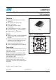
Figure 2. Electrical characteristics (T
amb
= 25 °C)
Table 2. Thermal resistance
Symbol Parameter Value Unit
R
th (j-a)
Junction to ambient 170 °C/W
V
RM
V
R
I
PP
I
H
I
R
I
RM
V
F
I
V
Symbol Parameter
I
GT
Gate triggering current
I
H
Holding current
I
RM
Reverse leakage current line / GND
I
RG
Reverse leakage current gate / line
V
RM
Reverse voltage line / GND
V
GT
Gate triggering voltage
V
F
Forward drop voltage line / GND
V
FP
Peak forward voltage line / GND
V
DGL
Dynamic switching voltage gate / Line
V
GATE
Gate / Gnd voltage
V
RG
Reverse voltage gate / Line
C Capacitance line / GND
Table 3. Absolute ratings (T
amb
= 25 °C, unless otherwise specified)
Symbol Parameter Value Unit
I
PP
Peak pulse current
(1)
10/1000 µs
8/20 µs
10/560 µs
5/310 µs
10/160 µs
1/20 µs
2/10 µs
20
60
20
25
30
60
70
A
I
TSM
Non repetitive surge peak on-state
current (50 Hz sinusoidal)
t = 10 ms
t = 1 s
5
3.5
A
I
2
tI
2
t value for fusing (50 Hz sinusoidal) t = 10 ms 0.125 A
2
s
I
GSM
Maximum gate current (50 Hz sinusoidal) t = 10 ms 2 A
V
MLG
V
MGL
Maximum voltage LINE/GND
Maximum voltage GATE/LINE
-40 °C < T
amb
< +85 °C
-40 °C < T
amb
< +85 °C
-150
-150
V
T
stg
T
j
Storage temperature range
Maximum junction temperature
- 55 to + 150
150
°C
T
L
Maximum lead temperature for soldering during 10 s 260 °C
1. For pulse waveform see Figure 3.