
Data Sheet
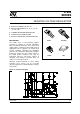


L7900 SERIES
7/18
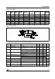
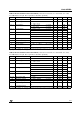
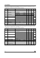
Table 11: Electrical Characteristics Of L7924C (refer to the test circuits, T
J
= 0 to 125°C, V
I
= -33V,
I
O
= 500 mA, C
I
= 2.2 µF, C
O
= 1 µF unless otherwise specified).
(*) Load and line regulation are specified at constant junction temperature. Changes in V
O
due to heating effects must be taken into account
separately. Pulse testing with low duty cycle is used.
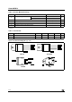
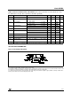
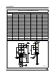
APPLICATIONS INFORMATION
Figure 4: Fixed Output Regulator
NOTE:
1. To specify an output voltage, substitute voltage value for "XX".
2. Required for stability. For value given, capacitor must be solid tantalum. If aluminium electrolytics are used, at least ten times value should
be selected. C1 is required if regulator is located an appreciable distance from power supply filter.
3. To improve transient response. If large capacitors are used, a high current diode from input to output (1N4001 or similar) should be intro-
duced to protect the device from momentary input short circuit.
Symbol Parameter Test Conditions Min. Typ. Max. Unit
V
O
Output Voltage T
J
= 25°C -23 -24 -24.5 V
V
O
Output Voltage I
O
= -5 mA to -1 A P
O
≤ 15 W
V
I
= -27 to -38 V
-22.8 -24 -25.2 V
∆V
O
(*) Line Regulation V
I
= -27 to -38 V T
J
= 25°C 480 mV
V
I
= -30 to -36 V T
J
= 25°C 240
∆V
O
(*) Load Regulation I
O
= 5 mA to 1.5 A T
J
= 25°C 480 mV
I
O
= 250 to 750 mA T
J
= 25°C 240
I
d
Quiescent Current T
J
= 25°C 3 mA
∆I
d
Quiescent Current Change I
O
= 5 mA to 1 A 0.5 mA
V
I
= -27 to -38 V 1
∆V
O
/∆T Output Voltage Drift I
O
= 5 mA -1 mV/°C
eN Output Noise Voltage B = 10Hz to 100KHz T
J
= 25°C 400 µV
SVR Supply Voltage Rejection ∆V
I
= 10 V f = 120Hz 54 60 dB
V
d
Dropout Voltage I
O
= 1 A T
J
= 25°C ∆V
O
= 100
mV
1.1 V
I
sc
Short Circuit Current 1.1 A