
Datasheet


Functional description L6480
34/75 DocID023278 Rev 4
6.18 Supply management and internal voltage regulators
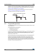
The L6480 integrates two linear voltage regulators: the first one can be used to obtain gate
driver supply starting from a higher voltage (e.g. the motor supply one). Its output voltage
can be set to 7.5 V or 15 V according to the VCCVAL bit value (CONFIG register). The
second linear voltage regulator can be used to obtain the 3.3 V logic supply voltage.
The regulator is designed to supply the internal circuitry of the IC and should not be used to
supply external components.
The input and output voltages of both regulators are connected to external pins and the
regulators are totally independent: in this way a very flexible supply management can be
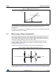
performed using external components or external supply voltages (Figure 15).
Figure 15. Device supply pin management
If V
CC
is externally supplied, the VSREG and VCC pins must be shorted (V
SREG
must be
compliant with V
CC
range).
If V
REG
is externally supplied, the VCCREG and VREG pins must be shorted and equal to
3.3 V.
V
SREG
must be always less than V
BOOT
in order to avoid related ESD protection diode turn-
on. The device can be protected from this event by adding an external low drop diode
between the VSREG and VS pins, charge pump diodes should be low drop too.
V
CCREG
must be always less than V
CC
in order to avoid ESD protection diode turn-on. The
device can be protected from this event by adding an external low drop diode between the
VCCREG and VSREG pins.
Both regulators provide a short circuit protection limiting the load current within the
respective maximum ratings.
9%227
&3
96
965(*
9&&
9&&5(*
95(*
99
9
9%227
&3
96
965(*
9&&
9&&5(*
95(*
99
9
9%86
8VLQJH[WHUQDOFRPSRQHQWV
]HQHUGLRGHVUHVLVWRUVLW
LVSRVVLEOHWRUHGXFHLQWHUQDO
SRZHUGLVVLSDWLRQFRQVWUDLQV
9%86
9&&
9
$OOYROWDJHVDUHLQWHUQDOO\JHQHUDWHG $OOYROWDJHVDUHH[WHUQDOO\VXSSOLHG
$0Y