
Datasheet


DocID023278 Rev 4 17/75
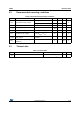
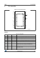
L6480 Pin connection
75
4 Pin connection
Pin list
Figure 2. Pin connection (top view)
9&&5(*
9&&
&3
9%227
3*1'
$'&,1
1&
+9*$
/9*$
287$
+9*%
287%
/9*%
96
965(*
95(*
26&,1
26&287
$*1'
9'',2
6:
67&.
'*1'
6'2
6',
&.
(3$'
+9*$
3*1'
3*1'
/9*$
287$
+9*%
287%
/9*%
&6
)/$*
67%<5(6(7
%86<6<1&
$0Y
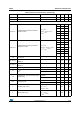
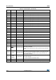
Table 6. Pin description
No. Name Type Function
11 VCCREG Power supply Internal V
REG
voltage regulator supply voltage
13 VREG Power supply Logic supply voltage
27 VDD Power supply Logic interface supply voltage
12 VSREG Power supply Internal V
CC
voltage regulator supply voltage
10 VCC Power supply Gate driver supply voltage
14 OSCIN Analog input Oscillator pin1. To connect an external oscillator or clock source.
15 OSCOUT Analog output
Oscillator pin2. To connect an external oscillator. When the internal
oscillator is used, this pin can supply a 2/4/8/16 MHz clock.
9 CP Output Charge pump oscillator output
7 VBOOT Power supply
Bootstrap voltage needed for driving the high-side power DMOS of
both bridges (A and B).
5 ADCIN Analog input Internal analog to digital converter input