
Datasheet


Electrical characteristics L6480
16/75 DocID023278 Rev 4
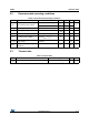
Standby
I
STBY
Standby mode supply current (VSREG
pin)
V
CC
= V
CCREG
= 7.5 V
V
SREG
= 48 V
42
µA
VCC = VCCREG = 7.5 V
V
SREG
= 18 V
37.5
I
STBY,vreg
Standby mode supply current (VREG pin) 6 µA
t
STBY,min
Minimum standby time 0.5 ms
t
logicwu
Logic power-on and wake-up time 500 µs
t
cpwu
Charge pump power-on and wake-up time
Power bridges disabled,
C
p
= 10 nF, C
boot
= 220 nF,
V
CC
= 15 V
1ms
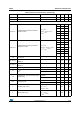
Internal voltage regulators
V
CCOUT
Internal V
CC
voltage regulator output
voltage
Low (default), I
CC
= 10 mA 7.3 7.5 V
High, I
CC
= 10 mA 14 15
V
SREG, drop
V
SREG to
V
CC
dropout voltage I
CC
= 50 mA 3 V
P
CC
Internal V
CC
voltage regulator power
dissipation
2.5 W
V
REGOUT
Internal V
REG
voltage regulator output
voltage
I
REG
= 10 mA 3.135 3.3 V
V
CCREG, drop
V
CCREG
to
V
REG
dropout voltage I
REG
= 50 mA 3 V
I
REGOUT
Internal V
REG
voltage regulator output
current
VREG pin shorted to
ground.
125 mA
I
REGOUT,STBY
Internal V
REG
voltage regulator output
standby current
VREG pin shorted to
ground.
55 mA
P
REG
Internal V
REG
voltage regulator power
dissipation
0.5 W
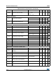
Integrated analog to digital converter
N
ADC
Analog to digital converter resolution 5 bit
V
ADC,ref
Analog to digital converter reference
voltage
3.3 V
f
S
Analog to digital converter sampling
frequency
(2)
f
PWM
kHz
V
ADC,UVLO
ADCIN UVLO threshold 1.05 1.16 1.35 V
1. Guaranteed in the temperature range -25 to 125 °C.
2. The value accuracy is dependent on oscillator frequency accuracy (Section 6.8 on page 27).
3. FLAG
and BUSY open drain outputs included.
4. See Figure 19 on page 41.
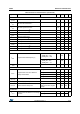
Table 5. Electrical characteristics (continued)
Symbol Parameter Test condition Min. Typ. Max. Unit