
Datasheet
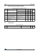


Electrical characteristics L6480
14/75 DocID023278 Rev 4
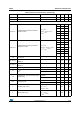
SRgate Gate driver output slew rate
I
GATE
= 96 mA
V
CC
= 15 V
C
GATE
= 15 nF
6V/s
Deadtime and blanking
t
DT
Programmable deadtime
2
TDT = '00000' 125
ns
TDT = ’11111’ 4000
t
blank
Programmable blanking time
2
TBLANK = '000' 125
ns
TBLANK = ’111’ 1000
Logic
V
IL
Low level logic input voltage 0.8 V
V
IH
High level logic input voltage 2 V
I
IH
High level logic input current V
IN
= 5 V, VDDIO = 5 V 1 µA
I
IL
Low level logic input current V
IN
= 0 V, VDDIO = 5 V -1 µA
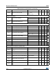
V
OL
Low level logic output voltage
(3)
V
DD
= 3.3 V, I
OL
= 4 mA 0.3
V
V
DD
= 5 V, I
OL
= 4 mA 0.3
V
OH
High level logic output voltage
V
DD
= 3.3 V, I
OH
= 4 mA 2.4
V
V
DD
= 5 V, I
OH
= 4 mA 4.7
R
PUCS
CS pull-up resistor 430
kR
PDRST
STBY/RESET pull-down resistor 450
R
PUSW
SW pull-up resistor 80
t
high,STCK
Step-clock input high time 300 ns
t
low,STCK
Step-clock input low time 300 ns
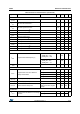
Internal oscillator and external oscillator driver
f
osc,int
Internal oscillator frequency T
j
= 25 °C -5% 16 +5% MHz
f
osc,ext
Programmable external oscillator
frequency
832MHz
V
OSCOUTH
OSCOUT clock source high level voltage Internal oscillator 2.4 V
V
OSCOUTL
OSCOUT clock source low level voltage Internal oscillator 0.3 V
t
rOSCOUT
t
fOSCOUT
OSCOUT clock source rise and fall time Internal oscillator 10 ns
t
high
OSCOUT clock source high time
Internal oscillator
62.5 ns
t
extosc
Internal to external oscillator switching
delay
3ms
t
intosc
External to internal oscillator switching
delay
100 µs
Table 5. Electrical characteristics (continued)
Symbol Parameter Test condition Min. Typ. Max. Unit