
Datasheet


DocID023278 Rev 4 13/75
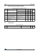
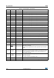
L6480 Electrical characteristics
75
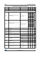
R
pumpLS
Charge pump low-side R
DS(ON)
resistance 10
I
boot
Average boot current 2.6 mA
Gate driver outputs
I
GATE,Sink
Programmable high-side and low-side
gate sink current
V
S
= 38 V
V
HVGX
- V
OUTX
> 3 V
V
LVGX
> 3 V
2.4 4 5.6
mA
5.4 8 10.6
11.3 16 20.7
17.3 24 30.7
23.2 32 40.8
50.2 64 77.8
81 96 113
I
GATE,Source
Programmable high-side and low-side
gate source current
V
S
= 38 V
V
BOOTX
- V
HVGX
> 3.5 V
V
CC
-V
LVGX
> 3.5 V
2.8 4 5.2
mA
5.8 8 10.2
12 16 20
18 24 30
24 32 40
51 64 77
82 96 112
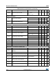
I
OB
High-side and low-side turn-off overboost
gate current
85 103 117 mA
R
CLAMP(LS)
Low-side gate driver Miller clamp
resistance
6.5 10
R
CLAMP(HS)
High-side gate driver Miller clamp
resistance
310
V
GATE-CLAMP
High-side gate voltage clamp I
GATE-CLAMP=10 mA
16.7 v
t
cc
Programmable constant gate current
time
(2)
TCC = ’00000’ 125
ns
TCC = 11111 3750
t
OB
Programmable. Turn-off overboost; gate
current time
(2)
TBOOST = ’001’, internal
oscillator
62.5 ns
TBOOST = ’111’ 1000
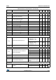
I
DSS
Leakage current
OUT = V
S
0.1 mA
OUT = GND -0.1 mA
t
r
Rise time (10% - 90%)
I
GATE
= 96 mA
V
CC
= 15 V
C
GATE
= 15 nF
2.5 s
t
f
Fall time (90%-10%)
I
GATE
= 96 mA
V
CC
= 15 V
C
GATE
= 15 nF
2.5 s
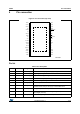
Table 5. Electrical characteristics (continued)
Symbol Parameter Test condition Min. Typ. Max. Unit