
Datasheet

Electrical data L6480
10/75 DocID023278 Rev 4
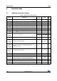
2 Electrical data
2.1 Absolute maximum ratings
Table 2. Absolute maximum ratings
Symbol Parameter
Test
condition
Value Unit
V
DD
Logic interface supply voltage 5.5 V
V
REG
Logic supply voltage 3.6
V
S
Motor supply voltage 95 V
V
CC
Low-side gate driver supply voltage 18 V
V
BOOT
Boot voltage 100 V
V
BOOT
High-side gate driver supply voltage 0 to 20 V
V
SREG
Internal V
CC
regulator supply voltage 95 V
V
CCREG
Internal V
REG
regulator supply voltage 18 V
V
OUT1A
V
OUT2A
V
OUT1B
V
OUT2B
Full bridge output voltage
DC -5 to V
BOOT
V
AC -15 to V
BOOT
SR
out
Full bridge outputs slew rate (10% - 90%) 10 V/ns
V
HVG1A
V
HVG2A
V
HVG1B
V
HVG2B
High-side output driver voltage V
OUT
to V
BOOT
V
V
HVG1A
V
HVG2A
V
HVG1B
V
HVG2B
High-side output driver to respective bridge output
voltage(V
HVG
- V
OUT
)
15 V
V
LVG1A
V
LVG2A
V
LVG1B
V
LVG2B
Low-side output driver voltage V
CC
+ 0.3 V
I
GATE-CLAMP
High-side gate voltage clamp current capability 100 mA
V
ADCIN
Integrated ADC input voltage range (ADCIN pin) -0.3 to 3.6 V
V
out_diff
Differential voltage between VBOOT, VS, OUT1A, OUT2A,
PGND and VBOOT, VS, OUT1B, OUT2B, PGND pins
100 V
V
in
Logic inputs voltage range -0.3 to 5.5 V
T
OP
T
s
Storage and operating junction -40 to 150 °C
P
tot
Total power dissipation (T
amb
= 25 ºC)
(1)
4W
1. HTSSOP38 mounted on a four-layer FR4 PCB with a dissipating copper surface of about 30 cm
2
.