
Datasheet


DocID023409 Rev 5 7/34
HVLED815PF Pin description and connection diagrams
34
2 Pin description and connection diagrams
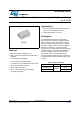
Figure 4. Pin connection (top view)
2.1 Pin description
N.A.
N.A.
N.A.
SOURCE
DRAIN
CS
GND
ILED
DMG
COMP
VCC
DRAIN
DRAIN
DRAIN
N.A.
1
2
3
4
5
6
7
8
16
15
14
13
12
11
10
9
N.C.
1
2
3
4
5
6
7
8
16
15
14
13
12
11
10
9
D
R
A
I
N
D
R
A
I
N
D
R
A
I
N
D
R
A
I
N
AM13210v1
Table 2. Pin description
No. Name Function
1 SOURCE Source connection of the internal power section.
2CS
Current sense input.
Connect this pin to the SOURCE pin (through an R
1
resistor) to sense the current flowing in the
MOSFET through an R
SENSE
resistor connected to GND. The CS pin is also connected
through dedicated R
OS
, R
PF
resistors to the input and auxiliary voltage, in order to modulate
the input current flowing in the MOSFET according to the input voltage and therefore achieving
a high power factor. See Section 4.11: High power factor implementation on page 26 for more
details.
The resulting voltage is compared with the voltage on the ILED pin to determine MOSFET turn-
off. The pin is equipped with 250 ns blanking time after the gate drive output goes high for
improved noise immunity. If a second comparison level located at 1 V is exceeded, the IC is
stopped and restarted after V
CC
has dropped below 5 V.
3VCC
Supply voltage of the device.
A capacitor, connected between this pin and ground, is initially charged by the internal high
voltage startup generator; when the device is running, the same generator keeps it charged in
case the voltage supplied by the auxiliary winding is not sufficient. This feature is disabled in
case a protection is tripped. A small bypass capacitor (100 nF typ.) to GND may be useful to
get a clean bias voltage for the signal part of the IC.