
Datasheet


Device description HVLED815PF
18/34 DocID023409 Rev 5
erroneously. This T
BLANK
blanking time is dependent on the voltage on COMP pin: it is
T
BLANK
= 30 µs for V
COMP
= 0.9 V, and decreases almost linearly down to T
BLANK
= 6 µs for
V
COMP
= 1.3 V.
The voltage on the pin is both top and bottom limited by a double clamp, as illustrated in the
internal diagram of the DMG block of Figure 14. The upper clamp is typically located
at 3.3 V, while the lower clamp is located at -60 mV. The interface between the pin and the
auxiliary winding will be a resistor divider. Its resistance ratio as well as the individual
resistance values will be properly chosen (see Section 4.6, Section 4.7 on page 22 and
Section 4.11 on page 26).
Please note that the maximum I
DMG
sunk/sourced current has to not exceed ±2 mA (AMR)
in all the V
IN
range conditions. No capacitor is allowed between DMG pin and the auxiliary
transformer.
The switching frequency is top limited below 166 kHz, as the converter's operating
frequency tends to increase excessively at light load and high input voltage.
A starter block is also used to start up the system, that is, to turn on the MOSFET during
converter power-up, when no or a too small signal is available on the DMG pin. The starter
frequency is 2 kHz if COMP pin is below burst mode threshold, i.e. 1 V, while it becomes
8 kHz if this voltage exceeds this value.
After the first few cycles initiated by the starter, as the voltage developed across the auxiliary
winding becomes large enough to arm the DMG circuit, MOSFET's turn-on will start to be
locked to transformer demagnetization, hence setting up QR operation. The starter is
activated also when the IC is in “Constant Current” regulation and the output voltage is not
high enough to allow the DMG triggering.
If the demagnetization completes - hence a negative-going edge appears on the DMG pin -
after a time exceeding time T
BLANK
from the previous turn-on, the MOSFET will be turned
on again, with some delay to ensure minimum voltage at turn-on. If, instead, the negative-
going edge appears before T
BLANK
has elapsed, it will be ignored and only the first
negative-going edge after T
BLANK
will turn-on the MOSFET. In this way one or more drain
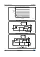
ringing cycles will be skipped (““valley-skipping mode”, Figure 15) and the switching
frequency will be prevented from exceeding 1/T
BLANK
.
Figure 15. Drain ringing cycle skipping as the load is progressively reduced
Note: That when the system operates in valley skipping-mode, uneven switching cycles may be
observed under some line/load conditions, due to the fact that the OFF-time of the MOSFET
is allowed to change with discrete steps of one ringing cycle, while the OFF-time needed for
cycle-by-cycle energy balance may fall in between. Thus one or more longer switching
cycles will be compensated by one or more shorter cycles and vice versa. However, this
mechanism is absolutely normal and there is no appreciable effect on the performance of
the converter or on its output voltage.
AM13565v1
P
in
= P
in''
< P
in'
P
in
= P
in'''
< P
in''
V
DS
T
FW
T
ON
V
DS
V
DS
T
OSC
T
OSC
T
OSC
P
in
= P
in'
(limit condition)
T
W
t t t