
Datasheet


DocID023409 Rev 5 11/34
HVLED815PF Electrical specifications
34
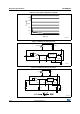
Figure 5. OFF-state drain and source current test circuit
Note: The measured I
DSS
is the sum between the current across the startup resistor and the
effective
MOSFET’s OFF-state drain current.
Current reference
V
ILEDx
Maximum value V
COMP
= V
COMPL
1.5 1.6 1.7 V
V
CLED
Current reference voltage
(6)
V
ILED
= 0.41 V, V
DMG
= 0 V;
T
J
= 25 °C
207.76 212 216.24 mV
Current sense
t
LEB
Leading-edge blanking
(5)
330 ns
T
D
Delay-to-output (H-L) 90 200 ns
V
CSx
Max. clamp value
(4)
dVcs/dt = 200 mV/µs 0.7 0.75 0.8 V
V
CSdis
Hiccup mode OCP level
(4)
0.92 1 1.08 V
1. V
CC
= 14 V (unless otherwise specified).
2. Limits are production tested at T
J
= T
A
= 25 °C, and are guaranteed by statistical characterization in the range
T
J
-25 to +125
°C.
3. Not production tested, guaranteed statistical characterization only.
4. Parameters tracking each other (in the same section).
5. Guaranteed by design.
6. Production tested only.
Table 5. Electrical characteristics
(1)
(2)
(continued)
Symbol Parameter Test condition Min. Typ. Max. Unit
2.5V
COMP SOURCE
DRAIN
VDD
+
-
CURR ENT
CONTROL
ILED
GND
DMG
CS
Vin
750V
A
Idss
14V
AM13211v1