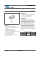
HVLED815PF Offline LED driver with primary-sensing and high power factor up to 15 W Datasheet - production data Applications AC-DC LED driver bulb replacement lamps up to 15 W, with high power factor AC-DC LED drivers up to 15 W Description SO16N Features High power factor capability (> 0.
Contents HVLED815PF Contents 1 2 3 4 Principle application circuit and block diagram . . . . . . . . . . . . . . . . . . . 4 1.1 Principle application circuit . . . . . . . . . . . . . . . . . . . . . . . . . . . . . . . . . . . . . 4 1.2 Block diagram . . . . . . . . . . . . . . . . . . . . . . . . . . . . . . . . . . . . . . . . . . . . . . . 6 Pin description and connection diagrams . . . . . . . . . . . . . . . . . . . . . . . 7 2.1 Pin description . . . . . . . . . . . . . . . . . . . . . .
HVLED815PF List of figures List of figures Figure 1. Figure 2. Figure 3. Figure 4. Figure 5. Figure 6. Figure 7. Figure 8. Figure 9. Figure 10. Figure 11. Figure 12. Figure 13. Figure 14. Figure 15. Figure 16. Figure 17. Figure 18. Figure 19. Figure 20. Figure 21. Figure 22. Figure 23. Figure 24. Figure 25. Application circuit for high power factor LED driver - single range input. . . . . . . . . . . . . . . . 4 Application circuit for standard LED driver . . . . . . . . . . . . . . . . . . . . . . . . .
Principle application circuit and block diagram 1.1 Principle application circuit Figure 1. Application circuit for high power factor LED driver - single range input Lin 1A_DIP 2 Cin 1 Lf CON1 8 J1 CON1 R12 C12 C13 Minimum Load 5 6 Cf Cout Bulk Cout SMD J3 CON1 TRANSFORMER Lf Rf CON1 VIN D5 U1 HVLED8xxPF Rsense 1 Rsense RA SOURCE DRAIN R1 (500 - 1.
HVLED815PF Figure 2. Application circuit for standard LED driver 1 1A_DIP 2 1 Lf Rsnubber F2 Csnubber + Bridge Diode Rf J7 Cin EMI FILTER 3 VIN CON1 9 3 4 8 J5 CON1 R18 C16 C27 Minimum Load 5 6 Cf Cout Bulk Cout SMD J6 CON1 TRANSFORMER 4 Lf Rf U2 HVLED8xxPF Rsense 1 Rsense SOURCE DRAIN 2 CS DRAIN VCC 3 C_Vcc (10uF) 4 C_ILED (10uF) 5 Rf b DMG 6 Rf (8.
Block diagram Figure 3. Block diagram + VIN VCC HV start-up & Supply Logic DRAIN LED Vref PROTECTION & FEEDFORWARD LOGIC DocID023409 Rev 5 DEMAG LOGIC RDMG RFB DMG DRIVING LOGIC CONSTANT CURRENT REGULATION Principle application circuit and block diagram 6/34 1.2 3.
HVLED815PF 2 Pin description and connection diagrams Pin description and connection diagrams Figure 4. Pin connection (top view) SOURCE 11 16 16 DRAIN CS 22 15 15 DRAIN VCC 33 14 14 DRAIN GND 44 13 13 DRAIN ILED 55 12 12 N.C. DMG 66 11 11 N.A. COMP 77 10 10 N.A. N.A. 88 9 N.A. AM13210v1 2.1 Pin description Table 2. Pin description No. 1 2 3 Name Function SOURCE Source connection of the internal power section. CS Current sense input.
Pin description and connection diagrams HVLED815PF Table 2. Pin description (continued) No. Name Function GND Ground. Current return for both the signal part of the IC and the gate drive. All of the ground connections of the bias components should be tied to a trace going to this pin and kept separate from any pulsed current return. ILED Constant current (CC) regulation loop reference voltage. An external capacitor CLED is connected between this pin and GND.
HVLED815PF Electrical specifications 3 Electrical specifications 3.1 Absolute maximum ratings Table 4. Absolute maximum ratings Symbol Pin Parameter Value Unit VDS 1, 13 - 16 Drain-to-source (ground) voltage -1 to 800 V ID 1, 13 - 16 Drain current(1) 1 A Eav 1, 13 - 16 Single pulse avalanche energy (TJ = 25 °C, ID = 0.7 A) 50 mJ VCC 3 Supply voltage (ICC < 25 mA) Self limiting V IDMG 6 Zero current detector current ±2 mA VCS 2 Current sense analog input -0.3 to 3.
Electrical specifications HVLED815PF Table 5. Electrical characteristics(1) (2) (continued) Symbol VCC_OFF VZ Parameter Test condition Min. Typ. Max. Unit 9 10 11 V 23 25 27 V See Figure 7 200 300 µA Quiescent current See Figure 8 1 1.4 mA Operating supply current at 50 kHz See Figure 9 1.4 1.
HVLED815PF Electrical specifications Table 5. Electrical characteristics(1) (2) (continued) Symbol Parameter Test condition Min. Typ. Max. Unit 1.5 1.6 1.7 V 207.76 212 216.24 mV Current reference VILEDx Maximum value VCLED VCOMP = VCOMPL (6) VILED = 0.41 V, VDMG = 0 V; TJ = 25 °C Current reference voltage Current sense tLEB Leading-edge blanking TD Delay-to-output (H-L) VCSx VCSdis (5) Max.
Electrical specifications HVLED815PF Figure 6. COSS output capacitance variation &RVV >S)@ 9GV > 9@ $0 Y Figure 7. Startup current test circuit Iccstart-up 11.8 V A VDD 2.5V DRAIN + CURRENT CONTROL - DMG ILED COMP GND SOURCE CS AM13213v1 Figure 8. Quiescent current test circuit Iq_meas A 14V VDD 2.5V DMG 33k 3V DRAIN + CURRENT CONTROL ILED COMP 0.8V GND CS SOURCE 10k 0.
HVLED815PF Electrical specifications Figure 9. Operating supply current test circuit Icc A 27k VDD 220k 2.5V DMG 10k DRAIN + CURRENT CONTROL ILED COMP 10k 1.5K 2W 15V GND CS 150V SOURCE 10 2.8V 5.6 -5V 50 kHz AM13215v1 Note: The circuit across the DMG pin is used for switch on synchronization. Figure 10. Quiescent current during fault test circuit Iq(fault) 14V A VDD 2.
Device description 4 HVLED815PF Device description The HVLED815PF device is a high voltage primary switcher intended for operating directly from the rectified mains with minimum external parts to provide high power factor (> 0.90) and an efficient, compact and cost effective solution for LED driving. It combines a highperformance low voltage PWM controller chip and an 800 V, avalanche rugged Power MOSFET, in the same package.
HVLED815PF Device description Moreover, the device is able to work in different modes depending on the LED's driver load condition (see Figure 11): 1. QR mode at heavy load. Quasi-resonant operation lies in synchronizing MOSFET's turn-on to the transformer's demagnetization by detecting the resulting negative-going edge of the voltage across any winding of the transformer. Then the system works close to the boundary between discontinuous (DCM) and continuous conduction (CCM) of the transformer.
Device description 4.3 HVLED815PF High voltage startup generator Figure 12 shows the internal schematic of the high voltage start-up generator (HV generator). It includes an 800 V-rated N-channel MOSFET, whose gate is biased through the series of a 12 M resistor and a 14 V Zener diode, with a controlled, temperature compensated current generator connected to its source. The HV generator input is in common with the DRAIN pins, while its output is the supply pin of the device (VCC pin).
HVLED815PF Device description Figure 13. Timing diagram: normal power-up and power-down sequences VIN VStart t VCC VccON Vccrestart t DRAIN t ICHARGE 5.5 mA Normal operation CV mode Power-on Normal operation CC mode Power-off t AM13563v1 Secondary side demagnetization detection and triggering block The demagnetization detection (DMG) and triggering blocks switch on the Power MOSFET if a negative-going edge falling below 50 mV is applied to the DMG pin.
Device description HVLED815PF erroneously. This TBLANK blanking time is dependent on the voltage on COMP pin: it is TBLANK = 30 µs for VCOMP = 0.9 V, and decreases almost linearly down to TBLANK = 6 µs for VCOMP = 1.3 V. The voltage on the pin is both top and bottom limited by a double clamp, as illustrated in the internal diagram of the DMG block of Figure 14. The upper clamp is typically located at 3.3 V, while the lower clamp is located at -60 mV.
HVLED815PF Constant current operation Figure 16 presents the principle used for controlling the average output current of the flyback converter. The voltage of the auxiliary winding is used by the demagnetization block to generate the control signal for the internal MOSFET switch Q. A resistor R in series with it absorbs a current equal to VILED/R, where VILED is the voltage developed across the capacitor CLED capacitor.
Device description HVLED815PF The capacitor CLED has to be chosen so that its voltage VILED can be considered as a constant. Since it is charged and discharged by currents in the range of some ten µA (IREF = 20 µA typ.) at the switching frequency rate, a capacitance value in the range 4.7 - 10 nF is suited for switching frequencies in the ten kHz. When high power factor schematic is implemented, a higher capacitor value should be used (i.e. 1 µF - 10 µF).
HVLED815PF Device description Equation 6 shows that the average output current IOUT does not depend anymore on the input voltage VIN or the output voltage VOUT, neither on transformer inductance values. The external parameters defining the output current are the transformer ratio n and the sense resistor RSENSE. Equation 6 is valid for both standard and high power factor implementation. 4.
Device description HVLED815PF Figure 18. Voltage control principle: internal schematic DMG + Aux EA + S/H - Rdmg 2.5V Rf b DEMAG LOGIC To PWM Logic CV From CS pin COMP R C AM13568v1 4.7 Voltage feedforward block The current control structure uses the VCLED voltage to define the output current, according to Equation 6 in Section 4.5.
HVLED815PF Device description Figure 19. Feedforward compensation: internal schematic DRAIN DMG Feedforward Logic . Rfb Aux IFF CC Block - Rdmg PWM LOGIC CC + Rff CS SOURCE Rsense AM13569v1 During MOSFET's ON-time the current sourced from DMG pin is mirrored inside the “Feedforward Logic” block in order to provide a feedforward current, IFF. Such “feedforward current” is proportional to the input voltage according to Equation 9: Equation 9 Where m is the primary-to-auxiliary turns ratio.
Device description HVLED815PF Equation 13 Finally, the RDMG resistor can be calculated as follows: Equation 14 In this case the peak drain current does not depend on input voltage anymore, and as a consequence the average output current IOUT does not depend from the VIN input voltage. When high power factor is implemented (see Section 4.
HVLED815PF Device description Figure 20. Load-dependent operating modes: timing diagrams COMP 50 mV hysteresis (Hys) VCOMPL IDS t Normal-mode Burst-mode Normal-mode t AM13570v1 4.9 Soft-start and starter block The soft-start feature is automatically implemented by the constant current block, as the primary peak current will be limited from the voltage on the CLED capacitor.
Device description HVLED815PF Ultimately, this will result in a low-frequency intermittent operation (hiccup mode operation), with very low stress on the power circuit. This special condition is illustrated in the timing diagram of Figure 21. Figure 21. Hiccup mode OCP: timing diagram VCC Secondary diode is shorted here VccON VccOFF Vccrest t VCS Vcsdis 1V VDS t Two switching cycles t AM13571v1 4.
HVLED815PF Device description Figure 22. High power factor implementation connection - single range input DRAIN DMG Feedf orward Logic1 . Rf b Aux IFF CC Block1 - Rdmg PWM LOGIC2 CC + Rf f CS SOURCE RPF R1 ROS VIN (after bridge diode) RA Rsense RB COS AM13572v1 The components selection flow starts from the RDMG resistor: this resistor has to be selected in order to minimize the internal feedforward effect.
Device description HVLED815PF The RA, RB, ROS resistors are selected to add a positive offset on CS pin in order to keep a good line regulation over the input voltage range and cab be selected using Equation 18: Equation 18 Where VOS_TYP is the desired voltage across COS capacitor applying the VIN_TYP typical input voltage (i.e.
HVLED815PF Device description Finally the current sense resistor RSENSE can be estimated in order to select the desiderated average output current value: Equation 24 where VCLED is internally defined (0.2 V typical - see Table 5: Electrical characteristics on page 9). System design tips Starting from the previous estimated components value, further fine-tuning on the real LED driver board could be necessary and it can be easily done considering that: 4.
Device description HVLED815PF Figure 23.
HVLED815PF 5 Package information Package information In order to meet environmental requirements, ST offers these devices in different grades of ECOPACK® packages, depending on their level of environmental compliance. ECOPACK specifications, grade definitions and product status are available at: www.st.com. ECOPACK is an ST trademark. Figure 24.
Package information HVLED815PF Table 6. SO16N package mechanical data Dimensions (mm) Symbol Min. Typ. A Max. 1.75 A1 0.10 A2 1.25 b 0.31 0.51 c 0.17 0.25 D 9.80 9.90 10.00 E 5.80 6.00 6.20 E1 3.80 3.90 4.00 e 0.25 1.27 h 0.25 0.50 L 0.40 1.27 k 0 8° ccc 0.10 Figure 25.
HVLED815PF 6 Revision history Revision history 22-Oct Table 7. Document revision history Date Revision 26-Jul-2012 1 Initial release. 29-Aug-2012 2 Added Table 2: Pin description on page 7. 3 Modified TJ value on Table 3: Thermal data. Updated TJ value in note 2 (below Table 5: Electrical characteristics). Minor text changes. 4 Added sections from 4.1 to 4.12.
HVLED815PF Please Read Carefully: Information in this document is provided solely in connection with ST products. STMicroelectronics NV and its subsidiaries (“ST”) reserve the right to make changes, corrections, modifications or improvements, to this document, and the products and services described herein at any time, without notice. All ST products are sold pursuant to ST’s terms and conditions of sale.