
Datasheet

ESDA14V2-1BF3 Characteristics
Doc ID 15894 Rev 1 3/9
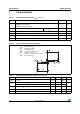
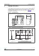
Figure 3. Relative variation of peak pulse
power versus initial junction
temperature
Figure 4. Peak pulse power versus
exponential pulse duration
0.0
0.1
0.2
0.3
0.4
0.5
0.6
0.7
0.8
0.9
1.0
1.1
0 25 50 75 100 125 150
P
PP
[T
j
initial] / P
PP
[T
j
initial=25°C]
T
j
(°C)
1
10
100
1000
1 10 100 1000
P
PP
(W)
T
j
initial = 25 °C
t
P
(µs)
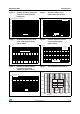
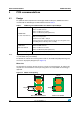
Figure 5. Clamping voltage versus peak
pulse current (square pulse,
typical values)
Figure 6. Junction capacitance versus
reverse applied voltage
(typical values)
0.1
1.0
10.0
15 16 17 18 19 20 21 22 23 24 25
I
PP
(A)
Square wave 2.5µs - T=25°C
V
CL
(V)
0
1
2
3
4
5
6
7
8
9
10
11
12
012345678910
C(pF)
F=1 MHz
V
OSC
=30mV
RMS
T
J
=25°C
Voltage(V)
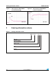
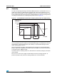
Figure 7. Relative variation of leakage
current versus junction
temperature (typical values)
Figure 8. S21 attenuation measurements
1
10
100
1000
25 50 75 100 125
I
R
[T
j
]/I
R
[T
j
=25°C]
V
R
=12V
T
j
(°C)
100.0k 1.0M 10.0M 100.0M 1.0G
-30.00
-24.00
-18.00
-12.00
-6.00
0.00
Attenuation
dB
F (Hz)
< -5.6dB
(-5.8dB@900MHz
-10.7dB@1.8GHz)
Attenuation
(0.8 – 4GHz)
505 MHz
-3 dB point
0.01 dB
Pass band
attenuation
Average
Performance
(50WSystem)
< -5.6dB
(-5.8dB@900MHz
-10.7dB@1.8GHz)
Attenuation
(0.8 – 4GHz)
505 MHz
-3 dB point
0.01 dB
Pass band
attenuation
Average
Performance
(50 Ω System)