
User Manual

© 2010 DiZiC Co. Ltd, 3F, N° 4-2 Jin Xi Street Taipei City 104, TAIWAN Email: info@dizic.com | Web: www.dizic.com
All Rights Reserved. All trademarks are property of their respective owners. Subject to change without notice.
Document ID: PB-ZB-MOD-003-20DS
4 ELECTRICAL CHARACTERISTICS
4.1 PARAMETER CONDITIONS
Unless otherwise specified, all voltages are referenced to VSS.
4.1.1 Minimum and maximum values
Unless otherwise specified the minimum and maximum values are guaranteed in the worst conditions of ambient temperature,
supply voltage and frequencies by tests in production on 100% of the devices with an ambient temperature at TA = 25 °C and
TA = TAmax (given by the selected temperature range). Data based on characterization results, design simulation and/or
technology characteristics are indicated in the table footnotes and are not tested in production. Based on characterization, the
minimum and maximum values refer to sample tests and represent the mean value plus or minus three times the standard
deviation (mean ±3σ).
4.1.2 Typical values
are given only as design guidelines and are not tested. Typical ADC accuracy values are determined by characterization of a
batch of samples from a standard diffusion lot over the full temperature range.
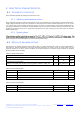
4.2 ABSOLUTE MAXIMUM RATINGS
Stresses above the absolute maximum ratings listed in Table 4.1: Voltage characteristics, Table 4.2: Current characteristics
and Table 4.3: Thermal characteristics may cause permanent damage to the device. These are stress ratings only and
functional operation of the device at these conditions is not implied. Exposure to maximum rating conditions for extended
periods may affect device reliability.
Table 4.1 Voltage characteristics
Ratings
Min.
Max.
Unit
Regulator input voltage (VDD_PADS)
-0.3
+3.6
V
RF Input Power (for max level for correct packet reception Receive characteristics)
RX signal into a lossless balun
15
dBm
Voltage on any GPIO (PA[7:0], PB[7:0], PC[7:0]), SWCLK, nRESET, VREG_OUT
-0.3
VDD_PADS +0.3
V
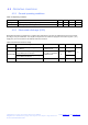
Table 4.2 Current characteristics
Symbol
Ratings
Max.
Unit
IVDD
Total current into VDD/VDDA power lines (source)
150
mA
IVSS
Total current out of VSS ground lines (sink)
150
mA
IIO
Output current sunk by any I/O and control pin
25
mA
Table 4.3 Thermal characteristics
Symbol
Ratings
Value
Unit
TSTG
Storage temperature range
–40 to +140
°C
TJ
Maximum junction temperature
150
°C