
User Manual

© 2010 DiZiC Co. Ltd, 3F, N° 4-2 Jin Xi Street Taipei City 104, TAIWAN Email: info@dizic.com | Web: www.dizic.com
All Rights Reserved. All trademarks are property of their respective owners. Subject to change without notice.
Document ID: PB-ZB-MOD-003-20DS
available with less than 1 μsec a power consumption while retaining RAM contents. To support user-defined applications, on-
chip peripherals include UART, SPI, TWI, ADC and general-purpose timers, as well as up to 24 GPIOs. Additionally, an
integrated voltage regulator, power-on-reset circuit, and sleep timer are available.
Finally, the STM32W utilizes standard Serial Wire and JTAG interfaces for powerful software debugging and programming of
the ARM Cortex-M3 core. The STM32W integrates the standard ARM system debug components: Flash Patch and Breakpoint
(FPB), Data Watch-point and Trace (DWT), and Instrumentation Trace Macrocell (ITM).
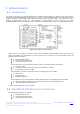
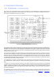
3.2 RF FRONT END WITH RF OUTPUT POWER LEVEL DETECTOR
The Front End (FE) is a fully integrated, single-chip, single-die microwave IC which incorporates all the RF functionality
needed for today’s wireless communications. The FE architecture integrates the PA, LNA, Transmit and Receive switching
circuitry, the associated matching network, and the harmonic filter -- all in a BiCMOS single-chip device. Combining superior
performance, high sensitivity and efficiency, low noise, small form factor, and low cost, is the perfect solution for applications
requiring extended range and bandwidth and can result in a potential 10x range increase. The RF power level (at PA output)
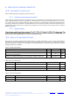
detect circuit is also integrated. Block diagram of the module with this FE is shown below:
Fig. 3.2 Block diagram of the module with front end incorporating RF power level detector (Power level option “R”)
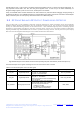
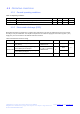
Functional description of the signals controlling front end are summarized in table 3.1 below
Table 3.1 Functional description of the Front End signals
FE Signal name
Direction
Description
STM32W108 port name
TX_ON
Digital input to FE
When RX_ON = 1:
TX_ON = 1: Transmit Mode
TX_ON = 0: Receive Mode
PC5, TX_ACTIVE
RX_ON
Digital input to FE
RX_ON = 0: FE in shut down mode
RX_ON = 1: FE enabled
Transmit / Receive function is determined by
TX_ON signal
PC6, nTX_ACTIVE
PA_DETECT
Analog output from FE
PA_DETECT voltage is proportional to
generated RF power at FE output pin.
For RF output power between:
+5 dBm to +20 dBm
PA_DETECT voltage is between
20 mV to 1200 mV respectively
PB5, ADC0