
User Manual

© 2010 DiZiC Co. Ltd, 3F, N° 4-2 Jin Xi Street Taipei City 104, TAIWAN Email: info@dizic.com | Web: www.dizic.com
All Rights Reserved. All trademarks are property of their respective owners. Subject to change without notice.
Document ID: PB-ZB-MOD-003-20DS
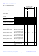
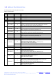
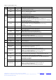
Table 5.1: Pad Description (cont)
Pad#
Signal
Direction
Description
31
PB7
I/O High current
Digital I/O
ADC2
Analog
ADC Input 2
Enable analog function with GPIO_PBCFGH[15:12]
IRQC1
I
Default external interrupt source C
TIM1_CH2
O
Timer 1 channel 2 output.
Enable timer output in TIM1_CCER.
Select alternate output function with GPIO_PBCFGH[15:12].
I
Timer 1 channel 2 input .(Cannot be remapped).
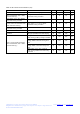
32
PB6
I/O High current
Digital I/O.
ADC1
Analog
ADC Input 1.
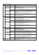
Enable analog function with GPIO_PBCFGH[11:8].
IRQB
I
External interrupt source B.
TIM1_CH1
O
Timer 1 channel 1 output.
Enable timer output in TIM1_CCER.
Select alternate output function with GPIO_PBCFGH[11:8].
I
Timer 1 channel 1 input. (Cannot be remapped).
33
PB5
I/O
Digital I/O
ADC0
Analog
ADC Input 0.
Enable analog function with GPIO_PBCFGH[7:4].
TIM2CLK
I
Timer 2 external clock input.
TIM1MSK
I
Timer 2 external clock mask input.
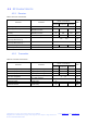
34
GND
Power
Ground supply pad.
35
GNDRF
RF Ground
Ground pad for RF port.
36
RF
Analog
RF port with 50 Ohm impedance.
37
GNDRF
RF Ground
Ground pad for RF port.
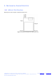
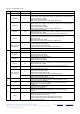
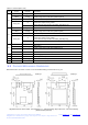
5.3 PACKAGE MECHANICAL DIMENSIONS
Module dimensions are 25 mm x 19 mm x 2 mm and detailed drawing is shown below on Fig. 5.2.
Fig. 5.2 Dimensions of the module. Left: EMI Option “S” -- without shielding; Right: Option “M” – with metal shielding
(Enhanced EMI protection)