
User Manual

© 2010 DiZiC Co. Ltd, 3F, N° 4-2 Jin Xi Street Taipei City 104, TAIWAN Email: info@dizic.com | Web: www.dizic.com
All Rights Reserved. All trademarks are property of their respective owners. Subject to change without notice.
Document ID: PB-ZB-MOD-003-20DS
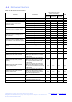
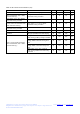
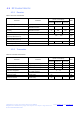
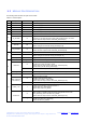
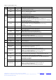
Table 5.1: Pad Description (cont)
Pad#
Signal
Direction
Description
15
PA2
I/O
Digital I/O.
TIM2_CH4 (see
also Pad 11)
O
Timer 2 channel 4 output.
Disable remap with TIM2_OR[7].
Enable timer output in TIM2_CCER .
Select alternate output function with GPIO_PACFGL[11:8].
I
Timer 2 channel 4 input Disable remap with TIM2_OR[7].
SC2SCL
I/O
TWI clock of Serial Controller 2.
Either disable timer output in TIM2_CCER, or enable remap with TIM2_OR[7].
Select TWI with SC2_MODE.
Select alternate open-drain output function with GPIO_PACFGL[11:8].
SC2SCLK
O
SPI master clock of Serial Controller 2.
Either disable timer output in TIM2_CCER, or enable remap with TIM2_OR[7].
Enable master with SC2_SPICFG[4].
Select SPI with SC2_MODE.
Select alternate output function with GPIO_PACFGL[11:8].
I
SPI slave clock of Serial Controller 2.
Enable slave with SC2_SPICFG[4].
Select SPI with SC2_MODE.
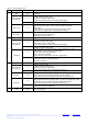
16
PA3
I/O
Digital I/O
SC2nSSEL
I
SPI slave select of Serial Controller 2
Enable slave with SC2_SPICFG[4]
Select SPI with SC2_MODE
TRACECLK (see
also Pad 27)
O
Synchronous CPU trace clock .
Either disable timer output in TIM2_CCER, or enable remap with TIM2_OR[5].
Enable trace interface in ARM core.
Select alternate output function with GPIO_PACFGL[15:12].
TIM2_CH2 (see
also Pad 21)
O
Timer 2 channel 2 output.
Disable remap with TIM2_OR[5].
Enable timer output in TIM2_CCER.
Select alternate output function with GPIO_PACFGL[15:12].
I
Timer 2 channel 2 input Disable remap with TIM2_OR[5].
17
PA4
I/O
Digital I/O.
ADC4
Analog
ADC Input 4 Select analogue function with GPIO_PACFGH[3:0].
PTI_EN
O
Frame signal of Packet Trace Interface (PTI).
Disable trace interface in ARM core.
Select alternate output function with GPIO_PACFGH[3:0].
TRACEDATA2
O
Synchronous CPU trace data bit 2.
Select 4-wire synchronous trace interface in ARM core.
Enable trace interface in ARM core.
Select alternate output function with GPIO_PACFGH[3:0].
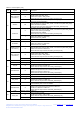
18
PA5
I/O
Digital I/O.
ADC5
Analog
ADC Inputs Select analog function with GPIO_PACFGH[7:4].
PTI_DATA
O
Data signal of Packet Trace Interface (PTI).
Disable trace interface in ARM core.
Select alternate output function with GPIO_PACFGH[7:4].
nBOOTMODE
I
Embedded serial boot-loader activation out of reset Signal is active during
and immediately after a reset on nRESET.
TRACEDATA3
O
Synchronous CPU trace data bit 3.
Select 4-wire synchronous trace interface in ARM core.
Enable trace interface in ARM core.
Select alternate output function with GPIO_PACFGH[7:4].
19
PA6
I/O High current
Digital I/O.
TIM1_CH3
O
Timer 1 channel 3 output.
Enable timer output in TIM1_CCER.
Select alternate output function with GPIO_PACFGH[11 :8].
I
Timer 1 channel 3 input Cannot be remapped.