
Data Sheet

BTA/BTB08 and T8 Series
6/10
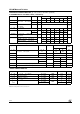
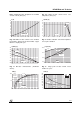
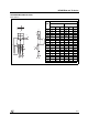
Fig. 6: Non-repetitive surge peak on-state
current for a sinusoidal pulse with width
tp < 10ms, and corresponding value of I²t.
Fig. 7: Relative variation of gate trigger current,
holding current and latching current versus
junction temperature (typical values).
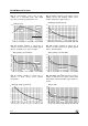
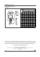
Fig. 8-1: Relative variation of critical rate of
decrease of main current versus (dV/dt)c (typical
values). Snubberless & Logic Level Types
Fig. 8-2: Relative variation of critical rate of
decrease of main current versus (dV/dt)c (typical
values). Standard Types
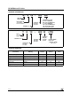
Fig. 9: Relative variation of critical rate of
decrease of main current versus junction
temperature.
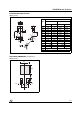
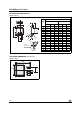
Fig. 10: DPAK and D
2
PAK Thermal resistance
junction to ambient versus copper surface under
tab (printed circuit board FR4, copper thickness:
35 µm).
0.01 0.10 1.00 10.00
10
100
1000
ITSM (A), I²t (A²s)
Tj initial=25°C
ITSM
I²t
dI/dt limitation:
50A/µs
tp (ms)
-40 -20 0 20 40 60 80 100 120 140
0.0
0.5
1.0
1.5
2.0
2.5
IGT,IH,IL[Tj] / IGT,IH,IL [Tj=25°C]
IGT
IH & IL
Tj(°C)
0.1 1.0 10.0 100.0
0.0
0.2
0.4
0.6
0.8
1.0
1.2
1.4
1.6
1.8
2.0
2.2
(dI/dt)c [(dV/dt)c] / Specified (dI/dt)c
T835/CW/BW
TW
T810/SW
(dV/dt)c (V/µs)
0.1 1.0 10.0 100.0
0.4
0.6
0.8
1.0
1.2
1.4
1.6
1.8
2.0
(dI/dt)c [(dV/dt)c] / Specified (dI/dt)c
C
B
(dV/dt)c (V/µs)
0 25 50 75 100 125
0
1
2
3
4
5
6
(dI/dt)c [Tj] / (dI/dt)c [Tj specified]
Tj(°C)
0 4 8 1216202428323640
0
10
20
30
40
50
60
70
80
90
100
Rth(j-a) (°C/W)
DPAK
D²PAK
S(cm²)