
Data Sheet
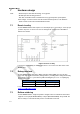
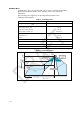
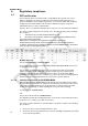

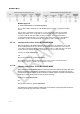
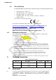
Table Of Contents

BLUENRG-M2Sx
13
7 Hardware design
Note: - All unused pins should be left floating; do not ground.
- All GND pins must be well grounded.
- The area around the module should be free of any ground planes, power planes,
trace routings, or metal for 6 mm from the module antenna position, in all directions.
- Traces should not be routed underneath the module.
7.1 Reset circuitry
The BLUENRG-M2Sx module requires an external pull-up reset circuitry to ensure proper
operation at power on. Refer to the "Reset management" chapter of the BlueNRG-2
datasheet for details.
If reset pin is controlled by an external host, there is no need to have RC circuit on the
RESETn line.
7.2 Debug interface
The BLUENRG-M2Sx embeds the ARM serial wire debug (SWD) port. It is two pins
(clock and single bi-directional data) debug interface, providing all the debug functionality
plus real time access to system memory without halting the processor or requiring any
target resident code.
Pin Functionality
Module PIN
Pin description
SWCLK
12
SWD clock signal
SWDIO
13
SWD data signal
For more information refer to the BlueNRG-2 technical documentation
(
www.st.com/BlueNRG-2.html)
7.3 Reflow soldering
The BLUENRG-M2Sx is a high temperature strength surface mount Bluetooth
®
module
supplied on a 23 pin (BLUENRG-M2SA) or 20 pin (BLUENRG-M2SP) 4-layer PCB. The
final assembly recommended reflow profiles are indicated here below.
Figure 10. Reset circuitry