
Datasheet

DocID15232 Rev 7 5/30
VIPER16 Pin settings
30
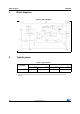
3 Pin settings
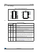
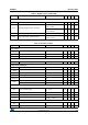
Figure 3. Connection diagram (top view)
Note: The copper area for heat dissipation has to be designed under the DRAIN pins.
$0Y
1&
1$
'5$,1
'5$,1
'5$,1
'5$,1
'5$,1
'5$,1
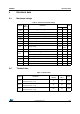
Table 3. Pin description
Pin N.
Name Function
DIP-7 SO16
11-2GND
Connected to the source of the internal power MOSFET and controller
ground reference.
-4N.A.
Not available for user. This pin is mechanically connected to the
controller die pad of the frame. In order to improve the noise immunity,
is highly recommended connect it to GND (pin 1-2).
2 5 VDD
Supply voltage of the control section. This pin provides the charging
current of the external capacitor.
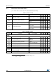
36LIM
This pin allows setting the drain current limitation to a lower value
respect to I
Dlim
, which is the default one. The limit can be reduced by
connecting an external resistor between this pin and GND. In case of
high electrical noise, a capacitor could be connected between this pin
and GND, the capacitor value must be lower than 470 nF in order to
not impact the functionality of the pin. The pin can be left open if
default drain current limitation, I
Dlim
, is used.
47FB
Inverting input of the internal trans conductance error amplifier.
Connecting the converter output to this pin through a single resistor
results in an output voltage equal to the error amplifier reference
voltage (see V
FB_REF
on Table 8). An external resistors divider is
required for higher output voltages.