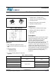
VIPER16 Fixed frequency VIPer™ plus family Datasheet - production data • Standby power < 30 mW at 230 VAC • Limiting current with adjustable set point • On-board soft-start • Safe auto-restart after a fault condition 62 QDUURZ • Hysteretic thermal shutdown ',3 Application Figure 1.
Contents VIPER16 Contents 1 Block diagram . . . . . . . . . . . . . . . . . . . . . . . . . . . . . . . . . . . . . . . . . . . . . . 4 2 Typical power . . . . . . . . . . . . . . . . . . . . . . . . . . . . . . . . . . . . . . . . . . . . . . . 4 3 Pin settings . . . . . . . . . . . . . . . . . . . . . . . . . . . . . . . . . . . . . . . . . . . . . . . . 5 4 Electrical data . . . . . . . . . . . . . . . . . . . . . . . . . . . . . . . . . . . . . . . . . . . . . . 7 4.1 Maximum ratings . . . . .
VIPER16 Contents 16 Layout guidelines and design recommendations . . . . . . . . . . . . . . . . 23 17 Package mechanical data . . . . . . . . . . . . . . . . . . . . . . . . . . . . . . . . . . . . 25 18 Revision history . . . . . . . . . . . . . . . . . . . . . . . . . . . . . . . . . . . . . . . . . . .
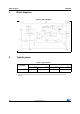
Block diagram 1 VIPER16 Block diagram Figure 2. Block diagram 2 Typical power Table 2. Typical power 85-265 VAC 230 VAC Part number VIPER16 Adapter(1) Open frame(2) Adapter(1) Open frame(2) 9W 10 W 5W 6W 1. Typical continuous power in non ventilated enclosed adapter measured at 50 °C ambient. 2. Maximum practical continuous power in an open frame design at 50 °C ambient, with adequate heat sinking.
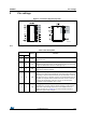
VIPER16 3 Pin settings Pin settings Figure 3. Connection diagram (top view) '5$,1 '5$,1 '5$,1 1 & '5$,1 1 $ '5$,1 '5$,1 $0 Y Note: The copper area for heat dissipation has to be designed under the DRAIN pins. Table 3. Pin description Pin N. Name Function 1-2 GND Connected to the source of the internal power MOSFET and controller ground reference. - 4 N.A. Not available for user. This pin is mechanically connected to the controller die pad of the frame.
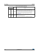
Pin settings VIPER16 Table 3. Pin description (continued) Pin N. DIP-7 6/30 Name Function COMP Output of the internal trans conductance error amplifier. The compensation network have to be placed between this pin and GND to achieve stability and good dynamic performance of the voltage control loop. The pin is used also to directly control the PWM with an optocoupler. The linear voltage range extends from VCOMPL to VCOMPH (Table 8). SO16 5 8 7,8 13-16 High voltage drain pin.
VIPER16 Electrical data 4 Electrical data 4.1 Maximum ratings Table 4. Absolute maximum ratings Parameter Unit Min VDRAIN 7, 8 Drain-to-source (ground) voltage EAV 7, 8 IAR Max 800 V Repetitive avalanche energy (limited by TJ = 150 °C) 2 mJ 7, 8 Repetitive avalanche current (limited by TJ = 150 °C) 1 A IDRAIN 7, 8 Pulse drain current (limited by TJ = 150 °C) 2.5 A VCOMP 5 Input pin voltage -0.3 3.5 V VFB 4 Input pin voltage -0.3 4.8 V VLIM 3 Input pin voltage -0.
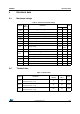
Electrical data 4.3 VIPER16 Electrical characteristics (TJ = -25 to 125 °C, VDD = 14 V (a); unless otherwise specified) Table 6. Power section Symbol Parameter Test condition IDRAIN = 1 mA, VCOMP = GND, TJ = 25 °C VBVDSS Break-down voltage RDS(on) Drain-source on state resistance COSS IOFF Min Typ Max Unit 800 IDRAIN = 0.2 A, TJ = 25 °C 20 24 Ω IDRAIN = 0.
VIPER16 Electrical data Table 7. Supply section (continued) Symbol Parameter Test condition Min Typ Max Unit Current IDD0 IDD1 Operating supply current, not switching Operating supply current, switching FOSC = 0 kHz, VCOMP = GND 0.6 mA VDRAIN = 120 V, FSW = 60 kHz 1.3 mA 1.5 mA 0.35 mA VDRAIN = 120 V, FSW = 115 kHz IDDoff Operating supply current with VDD < VDDoff VDD < VDDoff IDDol Open loop failure current threshold VDD = VDDclamp VCOMP = 3.3 V, 4 mA Table 8.
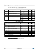
Electrical data VIPER16 Table 8. Controller section (continued) Symbol Parameter Test condition Min Typ Max Unit Oscillator section FOSC VIPer16L 54 60 66 kHz VIPer16H 103 115 127 kHz Switching frequency FD Modulation depth FM Modulation frequency DMAX Maximum duty cycle FOSC = 60 kHz ±4 kHz FOSC = 115 kHz ±8 kHz 230 Hz 70 80 % Thermal shutdown TSD THYST Thermal shutdown temperature(1) Thermal shutdown hysteresis(1) 1.
VIPER16 Typical electrical characteristics 5 Typical electrical characteristics Figure 4. IDlim vs TJ Figure 5. FOSC vs TJ ,' O LP ,' O LP# & ) 2 6& ) 2 6& # & $0 Y $0 Y Figure 6. VDRAIN_START vs TJ 7- >&@ 7- >&@ Figure 7.
Typical electrical characteristics VIPER16 Figure 10. ICOMP vs TJ Figure 11. Operating supply current (no switching) vs TJ ,& 2 0 3 , & 20 3# & ,' ' , '' # & 7- >&@ 7- >&@ $0 Y $0 Y Figure 12. Operating supply current (switching) vs TJ , '' ,' ' # & Figure 13. IDlim vs RLIM ,' O LP , ' OL P# .
VIPER16 Typical electrical characteristics Figure 16.
Typical circuit 6 VIPER16 Typical circuit Figure 17. Buck converter ' RSWLRQDO 5IE $& ,1 'LQ 5LQ / 9,3HU '5$,1 9'' 0 5IE )% & & &203 &IE & &21752/ & /,0 ' *1' 5FRPS &FRPS 5/,0 RSWLRQDO &/,0 RSWLRQDO /RXW 'RXW &RXW *5281' 9287 $0 Y Figure 18.
VIPER16 Typical circuit Figure 19. Flyback converter (primary regulation) $& ,1 )86( ' / & $& ,1 & 5FO &FO 9287 ' 5DX[ ' 'DX[ &RXW 5IEK 9,3HU '5$,1 9'' 0 )% &21752/ &9'' &203 /,0 *1' 5IEO &IE 5F &S &/,0 RSWLRQDO &F 5/,0 RSWLRQDO $0 Y Figure 20.
Power section 7 VIPER16 Power section The power section is implemented with an n-channel power MOSFET with a breakdown voltage of 800 V min. and a typical RDS(on) of 20 Ω. It includes a SenseFET structure to allow a virtually lossless current sensing and the thermal sensor. The gate driver of the power MOSFET is designed to supply a controlled gate current during both turn-ON and turn-OFF in order to minimize common mode EMI.
VIPER16 9 Oscillator Oscillator The switching frequency is internally fixed at 60 kHz (part number VIPER16LN or LD) or 115 kHz (part number VIPER16HN or HD).
FB pin and COMP pin 12 VIPER16 FB pin and COMP pin The device can be used both in non-isolated and in isolated topology. In case of nonisolated topology, the feedback signal from the output voltage is applied directly to the FB pin as inverting input of the internal error amplifier having the reference voltage, VREF_FB, see the Table 8 on page 9. The output of the error amplifier sources and sinks the current, ICOMP, respectively to and from the compensation network connected on the COMP pin.
VIPER16 Burst mode Figure 23. COMP pin voltage versus IDRAIN ,'5$,1 , 'OLP ,'OLPBEP 9&203/ 9&203+ 9&203 $0 Y 13 Burst mode When the voltage VCOMP drops below the threshold, VCOMPL, the power MOSFET is kept in OFF state and the consumption is reduced to IDD0 current, as reported on Table 7 on page 8.
Automatic auto restart after overload or short-circuit 14 VIPER16 Automatic auto restart after overload or short-circuit The overload protection is implemented in automatic way using the integrated up-down counter. Every cycle, it is incremented or decremented depending if the current logic detects the limit condition or not. The limit condition is the peak drain current, IDlim , reported on Table 8 on page 9 or the one set by the user through the RLIM resistor, as reported in Figure 13 on page 12.
VIPER16 Open loop failure protection In case the power supply is built in fly-back topology and the VIPer16 is supplied by an auxiliary winding, as shown in Figure 27 on page 21 and Figure 28 on page 22, the converter is protected against feedback loop failure or accidental disconnections of the winding. The following description is applicable for the schematics of Figure 27 on page 21 and Figure 28 on page 22, respectively the non-isolated fly-back and the isolated fly-back.
Open loop failure protection VIPER16 Figure 28.
VIPER16 16 Layout guidelines and design recommendations Layout guidelines and design recommendations A proper printed circuit board layout is essential for correct operation of any switch-mode converter and this is true for the VIPer16 as well. Also some trick can be used to make the design rugged versus external influences. Careful component placing, correct traces routing, appropriate traces widths and compliance with isolation distances are the major issues.
Layout guidelines and design recommendations VIPER16 Figure 29. Suggested routing for converter: flyback case 9287 $& $& *1' 9,3(5 9'' '5$,1 )% &21752/ &203 1 $ /,0 *1' 237,21$/ Figure 30.
VIPER16 17 Package mechanical data Package mechanical data In order to meet environmental requirements, ST offers these devices in different grades of ECOPACK® packages, depending on their level of environmental compliance. ECOPACK® specifications, grade definitions and product status are available at: www.st.com. ECOPACK® is an ST trademark. Figure 31.
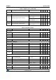
Package mechanical data VIPER16 Table 9. DIP-7 mechanical data mm Dim. Typ Min A 5,33 A1 0,38 A2 3,30 2,92 4,95 b 0,46 0,36 0,56 b2 1,52 1,14 1,78 c 0,25 0,20 0,36 D 9,27 9,02 10,16 E 7,87 7,62 8,26 E1 6,35 6,10 7,11 e 2,54 eA 7,62 eB L M (6)(8) N 10,92 3,30 2,92 3,81 0,40 0,60 2,508 0,50 N1 O (7)(8) 0,60 0,548 1- The leads size is comprehensive of the thickness of the leads finishing material.
VIPER16 Package mechanical data Figure 32.
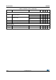
Package mechanical data VIPER16 Table 10. SO16N mechanical data mm Dim. Min Typ A 1.75 A1 0.1 A2 1.25 b 0.31 0.51 c 0.17 0.25 D 9.8 9.9 10 E 5.8 6 6.2 E1 3.8 3.9 4 e 0.25 1.27 h 0.25 0.5 L 0.4 1.27 k 0 8 ccc 28/30 Max 0.
VIPER16 18 Revision history Revision history s Table 11.
VIPER16 Please Read Carefully: Information in this document is provided solely in connection with ST products. STMicroelectronics NV and its subsidiaries (“ST”) reserve the right to make changes, corrections, modifications or improvements, to this document, and the products and services described herein at any time, without notice. All ST products are sold pursuant to ST’s terms and conditions of sale.