
Datasheet

VIPER06
Layout guidelines and design recommendations
DocID022794 Rev 2
21/28
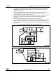
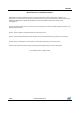
A small bypass capacitor (a few hundreds pF up to 0.1 µF) to GND might be useful to
get a clean bias voltage for the signal part of the IC and protect the IC itself during
EFT/ESD tests. A low ESL ceramic capacitor should be used, placed as close as
possible to the VDD pin;
When using SO16N package it is recommended to connect the pin 4 to GND pin,
using a signal track, in order to improve the noise immunity. This is highly
recommended in case of high nosily environment;
The IC thermal dissipation takes place through the drain pins. An adequate heat sink
copper area has to be designed under the drain pins to improve the thermal
dissipation;
It is not recommended to place large copper areas on the GND pins.
Minimize the area of the pulsed loops (primary, RCD and secondary loops), in order to
reduce its parasitic self- inductance and the radiated electromagnetic field: this will
greatly reduce the electromagnetic interferences produced by the power supply during
the switching.
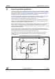
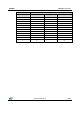
Figure 30: Suggested routing for converter: flyback case
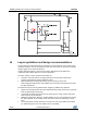
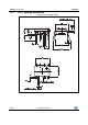
Figure 31: Suggested routing for converter: buck case