
Datasheet

Layout guidelines and design recommendations
VIPER06
20/28
DocID022794 Rev 2
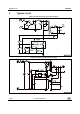
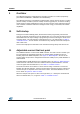
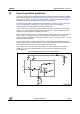
Figure 29: FB pin connection for isolated flyback
16 Layout guidelines and design recommendations
A proper printed circuit board layout is essential for correct operation of any switch-mode
converter and this is true for the VIPer06 as well. Also some trick can be used to make the
design rugged versus external influences.
Careful component placing, correct traces routing, appropriate traces widths and
compliance with isolation distances are the major issues.
The main reasons to have a proper PCB routing are:
Provide a noise free path for the signal ground and for the internal references,
ensuring good immunity against switching noises
Minimize the pulsed loops (both primary and secondary) to reduce the
electromagnetic interferences, both radiated and conducted and passing more easily
the EMC regulations.
The below list can be used as guideline when designing a SMPS using VIPer06.
Signal ground routing should be routed separately from power ground and, in general,
from any pulsed high current loop;
Connect all the signal ground traces to the power ground, using a single "star point",
placed close to the IC GND pin;
With flyback topologies, when the auxiliary winding is used, it is suggested to connect
the VDD capacitor on the auxiliary return and then to the main GND using a single
track;
The compensation network should be connected as close as possible to the COMP
pin, maintaining the trace for the GND as short as possible;