
Datasheet

FB pin and COMP pin
VIPER06
16/28
DocID022794 Rev 2
12 FB pin and COMP pin
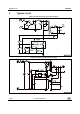
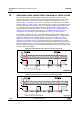
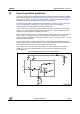
The device can be used both in non-isolated and isolated topology. In non-isolated
topology, the feedback signal from the output voltage is applied directly to the FB pin as the
inverting input of the internal error amplifier having the reference voltage, V
REF_FB,
see Table
7: "Controller section ".
The output of the error amplifier sources and sinks the current, I
COMP
, respectively to and
from the compensation network connected on the COMP pin. This signal is then compared
in the PWM comparator with the signal coming from the SenseFET in order to switch off
the power MOSFET on a cycle-by-cycle basis. See the Figure 2: "Block diagram" and the
Figure 23: "Feedback circuit".
When the power supply output voltage is equal to the error amplifier reference voltage,
V
REF_FB
, a single resistor has to be connected from the output to the FB pin. For higher
output voltages the external resistor divider is needed. If the voltage on the FB pin is
accidentally left floating, an internal pull-up protects the controller.
The output of the error amplifier is externally accessible through the COMP pin and it’s
used for the loop compensation, usually an RC network.
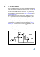
As shown in Figure 23: "Feedback circuit", in case of an isolated power supply, the internal
error amplifier has to be disabled (FB pin shorted to GND). In this case an internal resistor
is connected between an internal reference voltage and the COMP pin, see Figure 23:
"Feedback circuit". The current loop has to be closed on the COMP pin through the opto-
transistor in parallel with the compensation network. The V
COMP
dynamic range is between
V
COMPL
and V
COMPH
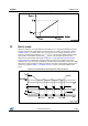
shown in Figure 24: "COMP pin voltage versus IDRAIN".
When the voltage V
COMP
drops below the voltage threshold V
COMPL
, the converter enters
burst mode, see Section 13: "Burst mode".
When the voltage V
COMP
rises above the V
COMPH
threshold, the peak drain current, as well
as the deliverable output power, will reach its limit.
Figure 23: Feedback circuit